
Solder Paste Inspection in PCBA: What SPI Catches Before Reflow and Why It Matters
SUNTOP Electronics
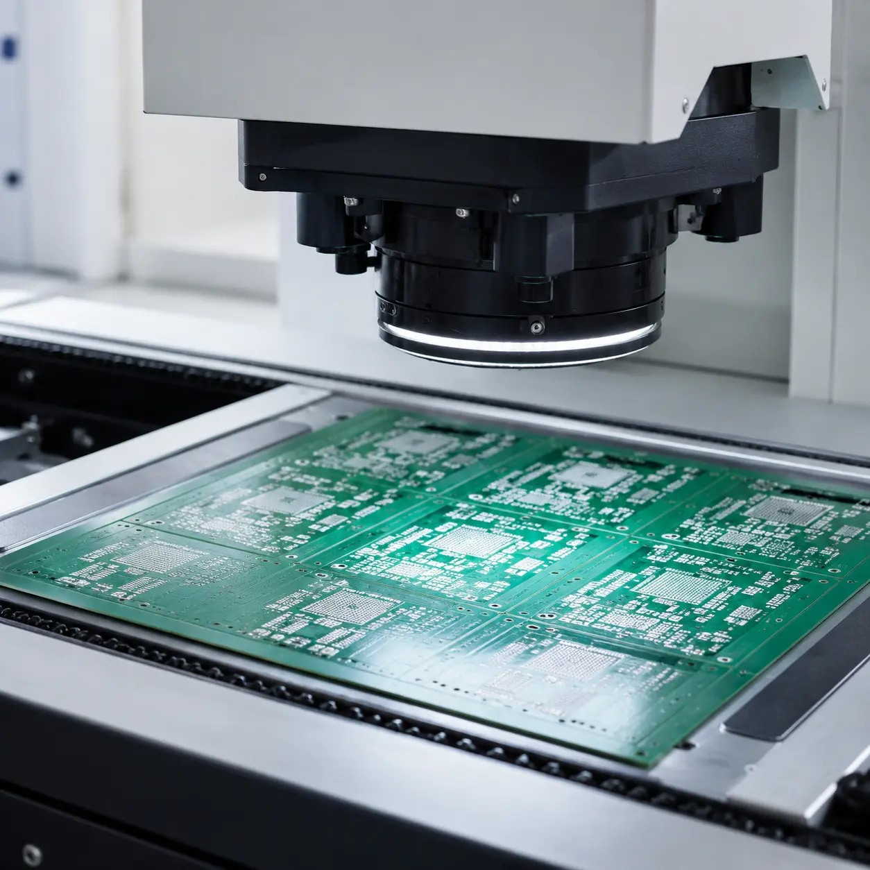
Solder paste inspection in PCBA is one of the clearest ways to catch assembly risk before a board ever reaches reflow. Instead of waiting until components are mounted and solder joints are already formed, the team checks the printed paste deposits while the board is still at the stencil-print stage.
That matters because many downstream defects start upstream. If paste volume is inconsistent, deposits are offset, apertures are underfilled, or bridging risk is visible before placement, those issues can be corrected earlier and at lower cost. A practical solder paste inspection in PCBA workflow helps manufacturing teams stop print-related defects before they turn into scrap, rework, or unstable process output.
This guide explains solder paste inspection in PCBA in practical terms for hardware teams, sourcing managers, and OEM buyers. It covers where SPI fits in the SMT flow, what it catches well, where it still has limits, and how to discuss SPI together with AOI and downstream test strategy when preparing a build.
What SPI Means and Where It Fits
At a simple level, solder paste inspection in PCBA means measuring or reviewing solder paste deposits on PCB pads after stencil printing and before component placement. The goal is to confirm that the printed paste pattern is close enough to the intended geometry, volume, and alignment for the board to move forward with less process risk.
In a normal surface-mount technology flow, stencil printing happens before pick-and-place and reflow. That makes SPI valuable because it gives the line an early control point. Instead of discovering a print problem only after solder joints are formed, the team can catch it while correction is still faster and cheaper.
This does not mean every line uses the same SPI method or intensity. Some programs apply tighter review on fine-pitch or high-density boards, while others use SPI more selectively around new product introduction, process changes, or known print-sensitive areas. The important point is that this inspection step is about pre-reflow print quality, not final product proof.
What SPI Catches Well Before Reflow
The real strength of solder paste inspection in PCBA is that it focuses on a defect source before components hide the evidence. When the printer, stencil, paste condition, and inspection program are aligned, SPI is very good at flagging issues such as:
- insufficient paste deposits on critical pads
- excess paste that raises bridging risk
- offset deposits that could affect component alignment
- missing deposits caused by clogging or print transfer issues
- shape irregularities that suggest stencil, support, or release problems
That is why SPI is so useful in NPI and in builds with tighter process windows. It does not wait for the reflow result to reveal that the print stage was unstable. It gives process engineers and quality teams a chance to react earlier.
For buyers, this matters because early print control supports more consistent assembly outcomes, especially on fine-pitch packages, small passive arrays, and denser SMT sections. SPI is one of the process-control layers worth understanding before the board reaches downstream inspection.
It is also helpful to remember that solder paste itself is a controlled manufacturing material, not just a generic consumable. Variables such as transfer behavior, stencil release, viscosity condition, and aperture design all affect what the SPI system is evaluating. A basic outside reference on solder paste is useful if your internal team needs a quick neutral refresher.
Limits of SPI and Why It Cannot Stand Alone
The biggest mistake teams make with solder paste inspection in PCBA is assuming that a good SPI result guarantees a good finished assembly. It does not.
SPI checks the print stage. It does not prove that components were placed correctly, that reflow created reliable solder joints, that hidden joints are acceptable, or that the board works electrically. A clean print can still be followed by placement errors, tombstoning, polarity mistakes, thermal imbalance, voiding concerns, or functional failures.
That is why solder paste inspection in PCBA should be described as early process control rather than complete inspection coverage. It is strongest when the main question is, “Did we print the paste correctly enough for this board to move into placement and reflow with confidence?” It is weaker when the question becomes, “Did the assembled board perform correctly in operation?”
This limit matters commercially as well. Buyers should not hear “SPI is included” and assume that all quality questions are closed. SPI is valuable, but it answers only one part of the broader assembly-risk picture.
Design and Process Factors That Affect SPI Results
Even a good machine cannot rescue a weak printing process by itself. SPI works best when board design, stencil strategy, and printer discipline are already reasonably controlled.
Several upstream factors influence the usefulness of the SPI data:
- pad geometry and spacing
- stencil thickness and aperture design
- board support during printing
- paste handling condition and print environment
- wipe frequency, clogging control, and printer setup stability
Dense boards with tight component spacing may need closer attention because small changes in deposit shape or volume matter more. Fine-pitch pads, bottom-terminated packages, and mixed-technology assemblies can also make print quality more sensitive to stencil design and process consistency.
This is one reason the discussion should start before the build, not after defects appear. If the board has print-sensitive areas, the supplier should know where they are and how much process margin the design really has.
When SPI Should Be Combined With AOI, ICT, or Functional Test
A strong verification plan is layered. Solder paste inspection in PCBA belongs near the start of that stack, but it should not be the only layer.
SPI checks print quality before placement and reflow. AOI checks visible assembly results after placement or reflow. If you want a deeper look at where optical review fits later in the line, this guide on AOI inspection in PCBA is the closest companion topic.
Electrical and behavioral methods answer different questions again. ICT helps verify electrical connectivity at accessible points, while functional test checks whether the assembled board behaves correctly in use. The broader ICT vs FCT vs AOI guide is useful when teams need to compare those roles without treating them as interchangeable labels.
In practice, the combination often looks like this:
- SPI for stencil-print verification before placement
- AOI for visible assembly defects after placement or reflow
- ICT or functional test where electrical behavior still needs confirmation
That layered approach is usually more credible than asking one inspection step to do every job.
How to Prepare a Better SPI Discussion With Your PCBA Supplier
The best conversations about solder paste inspection in PCBA are specific. Instead of asking only whether the inspection step is available, explain what kind of board you are building, which packages are most print-sensitive, and whether the build is prototype validation or repeat production.
A more useful supplier discussion usually includes:
- whether the board has fine-pitch or bottom-terminated packages
- whether stencil-print stability has been a past issue
- whether the build is NPI, pilot, or volume production
- whether AOI, ICT, or functional test will also be expected
- which areas of the board deserve tighter process attention
That kind of framing helps the supplier answer with process reality rather than generic marketing language. If your team wants to review inspection scope before a quote or build handoff, the project contact page is the right place to send board context and discuss how SPI fits the overall assembly plan.
FAQ About SPI in PCB Assembly
Is SPI the same as AOI?
No. SPI happens before component placement and focuses on printed paste deposits. AOI usually reviews visible assembly conditions after components are placed or soldered.
Does every SMT board need SPI?
Not every board needs the same level of SPI control, but this inspection step becomes more valuable when the board uses fine-pitch parts, dense layouts, or a tighter process window where print variation can create costly downstream defects.
Can SPI prove that the finished board will work?
No. SPI can confirm whether the print stage looks healthy, but it does not prove final electrical behavior, hidden-joint integrity, or product-level function.
Conclusion
Used well, solder paste inspection in PCBA helps teams catch print-related risk before it becomes harder and more expensive to correct. It is a practical upstream control step, especially for NPI work, fine-pitch assemblies, and programs where stencil-print consistency matters.
Used badly, it becomes another checkbox that sounds broader than it really is. The better approach is to treat SPI as an early process-control layer, combine it with downstream inspection and test where needed, and discuss its role clearly with the manufacturing partner before the build moves forward.