Smartphone PCB Assembly: Lessons from iPhone Repair
SUNTOP Electronics
Smartphone hardware is often discussed in terms of performance, thinness, battery life, and camera quality. But once a phone enters daily use, another reality takes over: screens crack, batteries degrade, charging ports wear out, connectors loosen, cameras stop responding, and some devices eventually need board-level repair or data recovery. For engineering teams, these field failures are not just after-sales events. They are a highly practical source of design and manufacturing insight.
A repair-focused website such as iPhone Station offers a useful public window into that reality. Its public-facing repair cases highlight recurring customer needs such as screen replacement, battery exchange, connector repair, camera repair, water-damage service, data recovery, and the buyback of devices with partial functional loss. Official repair documentation such as Apple Self Service Repair and community repair references such as iFixit’s iPhone repair guides also help show which smartphone subsystems repeatedly need service in the real world. That kind of public-facing repair pattern does not replace factory failure analysis, but it does reveal where smartphone-class products repeatedly experience stress after shipment.
For a PCB and PCBA manufacturer, that matters. The same issues that appear in repair shops are often linked to deeper questions in HDI PCB design, flex cable routing, fine-pitch connector strategy, BGA assembly quality, thermal management, and serviceability tradeoffs. In other words, repair demand is often the downstream expression of upstream electronics design and manufacturing decisions.
This article uses public repair patterns from iPhone-focused service ecosystems as an observation point, then brings the discussion back to what really matters for our audience: how to design and manufacture compact, reliable smartphone-class electronics more effectively.
Why Repair-Focused iPhone Sites Matter to PCB Engineers
At first glance, a repair website appears far removed from PCB manufacturing. It is built for consumers, not for engineers. But the categories featured on such sites are informative precisely because they represent repeat demand from real devices in circulation.
A site like iPhone Station prominently organizes its repair workflow and device purchase / trade-in flow around service demand such as:
- screen and display repair
- battery replacement
- camera-related repair
- connector replacement
- water-damage service
- data recovery
- used-device buyback, including damaged or partially defective devices
Those categories show where end users most often feel pain. For a hardware team, each of those issues maps to one or more underlying engineering layers:
- display issues may involve FPC connectors, driver circuits, impact loading, and board-to-board interconnect design
- battery service points to cycle aging, thermal conditions, power management layout, and assembly access constraints
- connector failures often reflect insertion wear, solder-joint stress, reinforcement design, and port mechanical protection
- water-damage cases expose weak points in sealing, corrosion resistance, contamination control, and layout sensitivity
- data-recovery or logic-board repair suggests the importance of HDI stack-up quality, rework risk, and hidden solder-joint reliability
That is why repair ecosystems are useful to study. They show not just what breaks, but what breaks often enough to justify an entire service workflow.
Smartphone Logic Boards Depend on HDI from the Beginning
Modern smartphones rely on a level of density that conventional PCB thinking cannot handle efficiently. Compared with many industrial or general consumer products, smartphone boards must support:
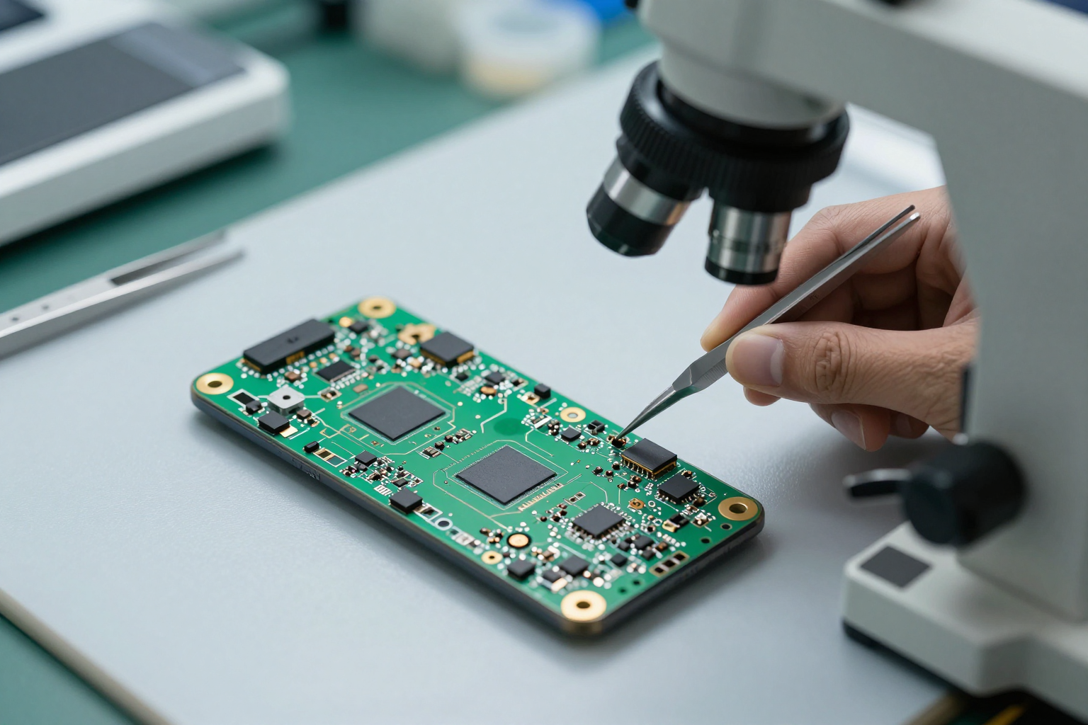
Smartphone-class logic boards rely on compact HDI architecture, where board density, connector zones, shielding, and fine-pitch package areas all raise the manufacturing difficulty level.
- extremely compact footprints
- multiple cameras and sensors
- high-speed interfaces
- RF subsystems
- dense power-management routing
- stacked or closely packed functional modules
- rigid-flex interconnection strategies
This is why smartphone logic boards are fundamentally tied to High-Density Interconnect (HDI) manufacturing. Fine trace/space rules, blind and buried vias, stacked microvias, thin dielectric control, and dense BGA fan-out are not optional luxuries in this product class. They are structural requirements.
As discussed in our article on the future of HDI PCB technology, HDI enables miniaturization and signal performance, but it also raises the difficulty level across fabrication, assembly, inspection, and rework. The more tightly packed the board becomes, the more every small variation matters:
- via integrity becomes more critical
- pad design becomes less forgiving
- reflow window control becomes tighter
- X-ray and electrical validation become more important
- field repair becomes more difficult and expensive
From a manufacturing perspective, smartphone-class HDI products require discipline at the stack-up level long before assembly starts. If the board design does not account for power density, heat distribution, connector zones, shielding requirements, and testability, the product may still launch — but it will accumulate expensive failure modes in the field.
Flex Cables and Connectors Are a Major Reliability Layer
Repair-oriented iPhone sites regularly feature services related to displays, cameras, buttons, and charging functions. On pages that group issues such as connector-related repair, the underlying pattern often points straight back to flex circuits and connectors.
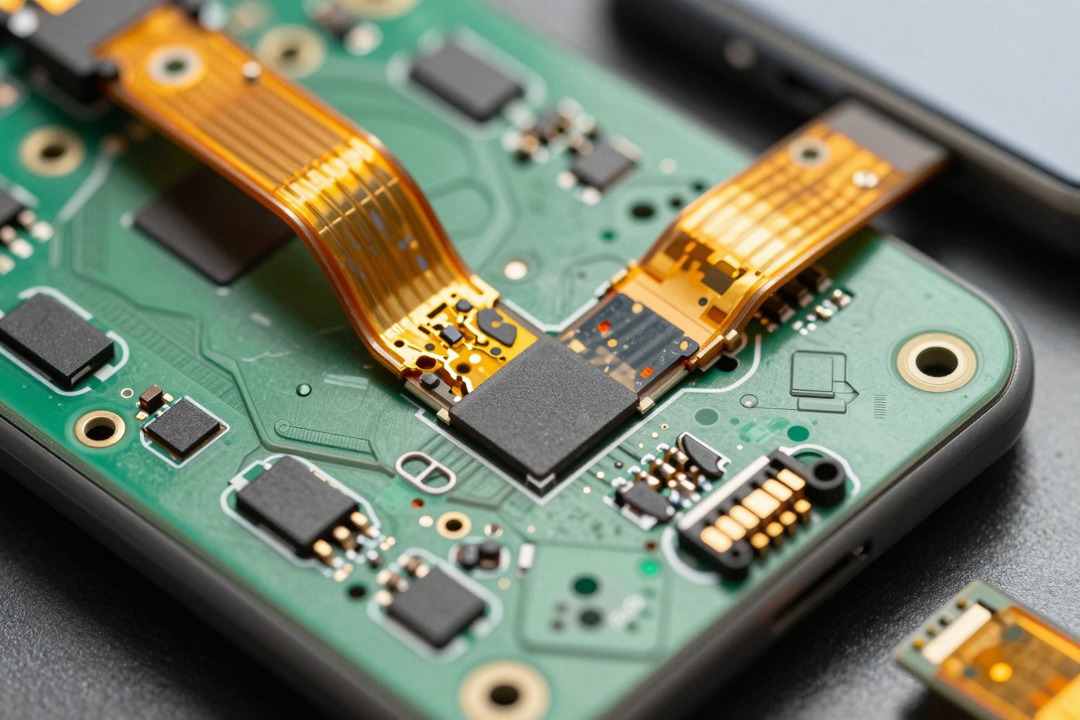
Flex assemblies and fine-pitch connectors often carry the real reliability burden in compact smartphones, where repeated stress, torsion, and service events can damage critical interconnect regions.
Many smartphone failures do not originate in the main logic board itself. They happen at the interfaces between subsystems:
- display FPCs
- camera module interconnects
- button flex assemblies
- dock or charging-port connectors
- board-to-board mating connectors
- battery and sensor harness transitions
In compact devices, these interfaces are subject to repeated mechanical and thermal stress. Drops, torsion, repeated cable movement during use or servicing, and everyday charging habits all contribute to gradual degradation. Even if the base PCB is designed well, poor connector retention strategy or weak flex transition design can dominate real-world repair rates.
That is why smartphone hardware teams should treat flex and connector design as first-class reliability topics rather than secondary packaging details. Our article on flexible PCB design best practices touches on several principles that become especially important in phones and other handheld devices:
- avoid excessive stress concentration at bend zones
- manage bend radius early in the layout phase
- reinforce high-load connector areas properly
- keep traces and copper geometry compatible with real movement patterns
- design with both manufacturing and later servicing in mind
A repair shop may describe a problem as “camera not working” or “charging issue,” but in many cases the deeper engineering story involves connector wear, flex fatigue, solder damage, or strain transfer into delicate interconnect regions.
Charging and Battery Repairs Reveal Power-Path Weaknesses
Battery replacement and charging-related repair are among the most visible categories on smartphone service sites, and for good reason. Public service pages for battery replacement and connector-related repair show how often those issues become customer-facing problems. The battery system is one of the highest-stress subsystems in a handheld product.
From a PCB assembly point of view, these cases raise several engineering questions:
1. Is the connector area mechanically protected?
Charging ports are repeatedly loaded by insertion, removal, cable leverage, accidental pulling, and side impact. If reinforcement strategy is weak, connector joints and surrounding pads become vulnerable.
2. Is the power-management region thermally balanced?
Heat accelerates aging. Battery replacement demand is not only a cell issue; it can also reflect power-path inefficiency, charging heat concentration, and enclosure-level thermal bottlenecks.
3. Are service events likely to damage adjacent assemblies?
On compact handheld boards, battery work can place secondary stress on nearby flexes, shields, adhesives, or board-to-board connectors. A manufacturable design is not automatically a service-friendly design.
4. Were the assembly process windows tight enough?
Fine-pitch power-management devices, battery connectors, and port assemblies require well-controlled soldering, inspection, and handling. Small inconsistencies in solder volume, coplanarity, or local heating can become field failures months later.
For smartphone-class electronics, the lesson is simple: power-path design must be treated as a combined system of electrical routing, mechanical stress, thermal behavior, and assembly execution.
Water Damage Is Really a Corrosion and Recovery Story
Another category commonly highlighted by repair services is water-damage repair and, in more severe cases, data recovery service. That category matters because moisture-related failures expose weaknesses that are not always obvious during standard production qualification.
Water ingress is not just an enclosure problem. Once liquids reach internal electronics, the risk expands into:
- corrosion around fine-pitch components
- contamination trapped under shields
- shorting across dense HDI features
- connector oxidation
- electrochemical damage in powered circuits
- latent reliability loss even after apparent recovery
For high-density smartphones, the recovery challenge is amplified by board compactness. Shield cans, underfilled components, tightly spaced passives, and dense stacked packages make cleaning, inspection, and rework much harder than on a larger or less integrated board.
That means manufacturers should think beyond “can the device survive a limited ingress event?” and also ask:
- how vulnerable are critical nets to localized contamination?
- how easy is it to inspect the highest-risk regions?
- how much hidden corrosion risk exists beneath dense assemblies?
- what parts of the design become effectively non-repairable after liquid exposure?
The more compact the device, the more water-damage service becomes a proxy for corrosion sensitivity and board recoverability.
Board-Level Repair Highlights BGA and Micro-Soldering Realities
Repair sites that mention logic-board work, data recovery, or devices with partial function loss point toward a different class of challenge: board-level repairability.
In smartphone products, that usually intersects with:
- fine-pitch BGAs
- underfilled devices
- dense shielding layouts
- stacked boards or split-board structures
- tightly packed passive networks
- limited access for probing and rework
Once a field failure reaches this level, the manufacturing implications become more serious. If the original assembly quality margin was narrow, the board may become extremely difficult to diagnose and recover outside a high-skill rework environment.
Our existing article on BGA assembly challenges and solutions explains why hidden solder joints require stronger process control, better inspection, and careful thermal profiling. In smartphone logic boards, those lessons become even more relevant because the package density is higher and repair access is worse.
The practical takeaway is that smartphone PCB assembly should not be optimized only for first-pass assembly efficiency. It should also be evaluated for:
- hidden joint reliability
- inspectability with X-ray and other methods
- risk concentration under shields
- local rework feasibility where possible
- probability of catastrophic pad damage during service
Not every product must be designed for board-level repair. But every serious hardware team should understand what repair shops reveal about the consequences of overly fragile assembly decisions.
What Hardware Teams Should Learn from iPhone Repair Patterns
For OEMs, startups, and engineering teams building compact consumer electronics, repair trends offer a valuable feedback loop. The most useful lesson is not “make devices easier to repair” in the abstract. The real lesson is to understand which subsystem decisions create avoidable downstream failure pressure.
Here are six practical design and manufacturing priorities that follow from smartphone repair patterns:
1. Treat connectors as reliability-critical components
Do not treat them as passive accessories in the BOM. Their pad design, reinforcement, retention, and local mechanical environment matter disproportionately.
2. Design flex transitions with real movement in mind
If a cable bends, folds, or sits near a stress concentration zone, that must be reflected in copper geometry, stiffener strategy, and physical routing.
3. Build HDI stack-ups for real thermal and mechanical life
A dense board that routes successfully in CAD may still accumulate stress around PMICs, RF modules, or memory packages under field conditions.
4. Plan inspection for hidden-risk areas
Phones contain too many hidden joints and too little access to rely on superficial visual confidence. X-ray, AOI, electrical test strategy, and process-window validation must be planned early.
5. Think about service impact even when service is not the main goal
Battery replacement, port wear, camera swap, and screen repair all place stress on nearby electronics. Service events are part of the real life of the product.
6. Choose a manufacturing partner that understands compact-electronics tradeoffs
Smartphone-class boards need more than generic PCB fabrication. They require a partner comfortable with HDI, fine-pitch SMT, flex integration, quality discipline, and component sourcing under tight dimensional constraints.
Why This Matters Beyond iPhones
Although this article uses iPhone repair patterns as the lens, the same lessons apply across many compact electronics segments:
- tablets and handheld scanners
- wearables and smartwatches
- portable medical devices
- camera modules and edge-AI devices
- rugged mobile terminals
- compact industrial HMIs
These products all compress more function into smaller spaces. As that happens, the distance between “minor field issue” and “serious board-level problem” becomes shorter. A connector weakness, a flex-routing oversight, or a thermal hotspot can quickly turn into a high-frequency service burden.
That is why smartphone assembly lessons matter even if you are not building a flagship phone. They are lessons about density, interfaces, stress, and manufacturing margin.
How a PCB and PCBA Partner Can Reduce Those Risks
At the design stage, many field failures still look hypothetical. At the repair stage, they become expensive facts. The role of a strong manufacturing partner is to reduce the gap between those two moments.
For smartphone-class and other compact products, that usually means support in five areas:
- HDI fabrication capability for dense routing and microvia structures
- fine-pitch SMT and BGA assembly for compact logic-board layouts
- flex and rigid-flex understanding for camera, display, and interconnect-heavy products
- component sourcing discipline for compact, high-turnover BOMs
- inspection and quality control depth for hidden joints and high-risk zones
At SUNTOP Electronics, we support this kind of build through integrated PCB fabrication, assembly, sourcing, and quality workflows. Teams working on compact consumer or handheld electronics often need not just a board vendor, but a partner who understands where manufacturability, reliability, and service risk intersect.
If your team is building smartphone-class hardware, these resources may help:
- The Future of HDI PCB Technology
- Flexible PCB Design: Key Considerations and Best Practices
- SMT PCB/FPC/HDI Assembly Guide
- BGA Assembly Challenges and Solutions
- 6 Step Quality Control Process
- PCB Manufacturing Capabilities
And if you are evaluating a compact, failure-sensitive design right now, you can contact our engineering team to review manufacturability, assembly risk, and prototype planning before volume production.
External References
For readers who want outside repair-context references behind this discussion, these two links are the most relevant:
Conclusion
A repair-focused website may seem far away from PCB manufacturing, but it often reveals what the field keeps trying to tell designers and manufacturers. Public repair patterns around screens, batteries, connectors, cameras, water damage, and data recovery all point back to the same reality: smartphone reliability is deeply tied to HDI quality, flex strategy, connector robustness, thermal behavior, and board-level assembly discipline.
That is the real lesson behind iPhone repair. What fails in service often begins as a design, stack-up, assembly, or inspection decision much earlier in the product lifecycle.
For teams building compact electronics, the smartest move is not to wait until repair demand exposes those weaknesses. It is to design and manufacture with those lessons already in mind.