PCB Assembly for Electronics: A Comprehensive Guide to Modern Manufacturing
Winnie King
In today’s hyper-connected world, nearly every electronic device relies on a printed circuit board (PCB) to function. From smartphones and laptops to medical equipment and automotive systems, PCB assembly for electronics is the critical process that brings these devices to life. It transforms bare circuit boards into fully functional components by precisely placing and soldering electronic parts.
Understanding PCB assembly for electronics is essential for engineers, product designers, and manufacturers aiming to deliver reliable, high-performance products. This guide explores the intricacies of the process, key technologies involved, quality assurance methods, and how choosing the right partner can make all the difference.
What Is PCB Assembly for Electronics?
PCB assembly for electronics refers to the process of mounting and connecting electronic components onto a printed circuit board. Unlike PCB fabrication—which focuses on creating the physical board with copper traces—assembly involves adding active and passive components such as resistors, capacitors, integrated circuits (ICs), and connectors.
This stage is where functionality is realized. Without accurate PCB assembly for electronics, even the most meticulously designed circuit remains inert. The assembled board, often referred to as a PCBA (Printed Circuit Board Assembly), becomes the operational core of any electronic system.
There are two primary methods used in PCB assembly for electronics: Surface Mount Technology (SMT) and Through-Hole Technology (THT). Each has its advantages depending on the application, component types, and performance requirements.
Key Methods in PCB Assembly for Electronics
Surface Mount Technology (SMT)
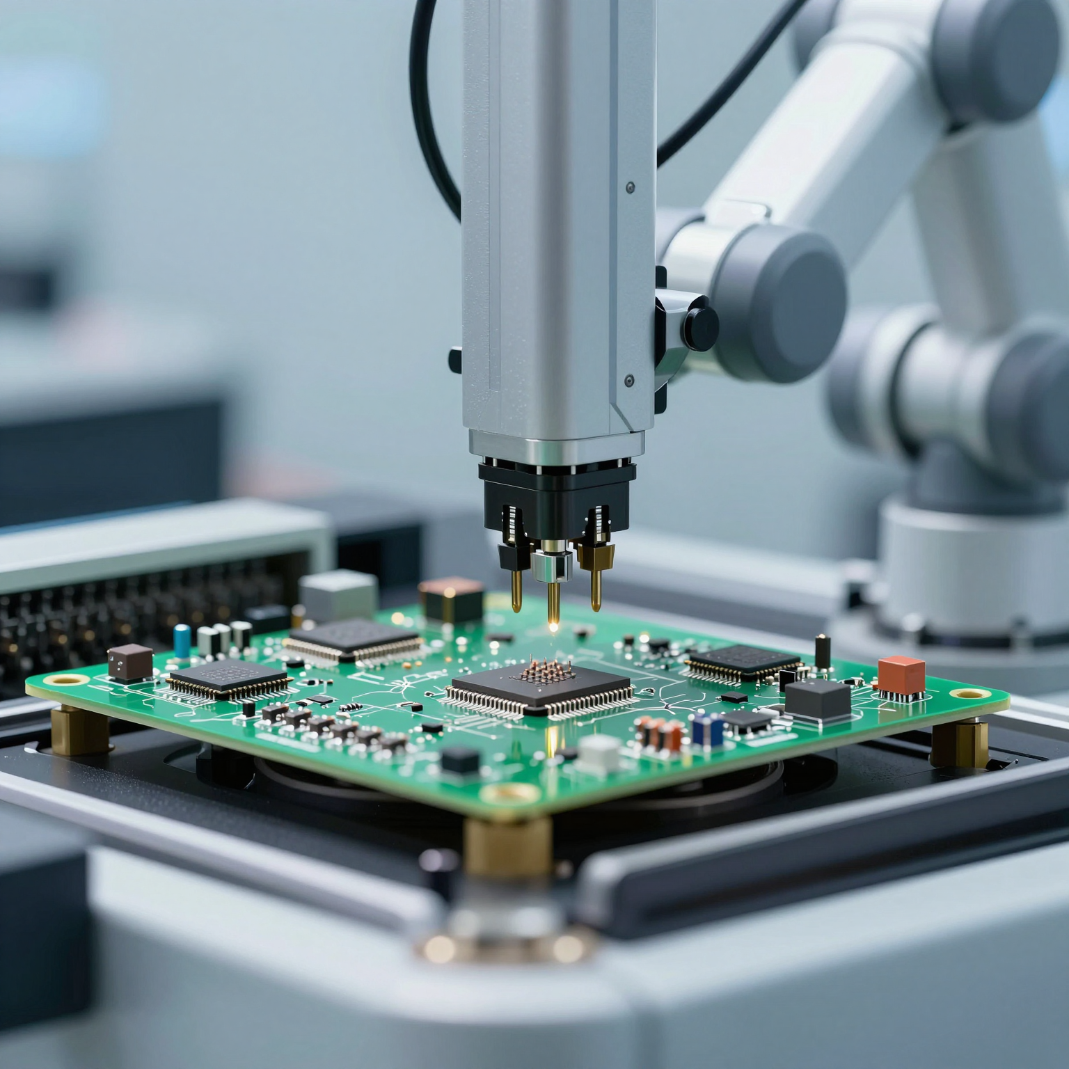
SMT dominates modern PCB assembly for electronics due to its efficiency, compactness, and suitability for automated production. In this method, components are placed directly onto the surface of the PCB and then soldered using reflow ovens.
The SMT process typically includes:
- **Solder Paste Application
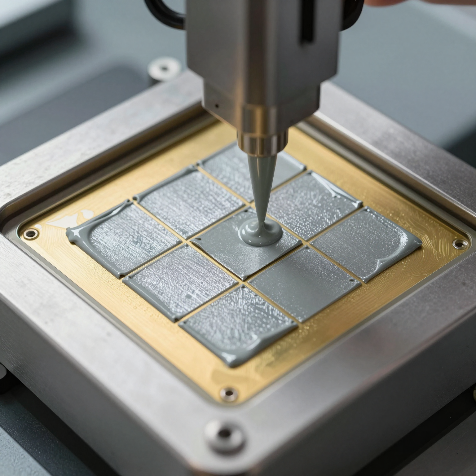
**: A stencil applies solder paste to the pads where components will be mounted. 2. **Component Placement
**: High-speed pick-and-place machines position components with extreme precision. 3. Reflow Soldering: The board passes through a reflow oven, melting the solder paste and forming electrical and mechanical connections.
SMT allows for smaller components and higher component density, making it ideal for consumer electronics like smartphones and wearables. For more details on how SMT compares to other techniques, read our article on SMT vs through-hole assembly. For a deep dive into the technology itself, check out this overview of Surface Mount Technology.
Through-Hole Technology (THT)
While less common in mass production, THT remains vital in applications requiring robust mechanical bonds. Components have leads that are inserted through holes drilled in the PCB and then soldered on the opposite side, usually via wave soldering.
THT is often used for larger components such as transformers, connectors, and power semiconductors. Although slower and more labor-intensive than SMT, it offers superior durability under stress, vibration, or extreme temperatures—making it suitable for aerospace, military, and industrial equipment.
Many advanced assemblies use a hybrid approach, combining both SMT and THT to leverage the strengths of each method within the same PCB assembly for electronics workflow.
Advanced Technologies Shaping PCB Assembly for Electronics
As electronic devices become smaller, faster, and more complex, PCB assembly for electronics must evolve accordingly. Several cutting-edge technologies are driving innovation in this space.
High-Density Interconnect (HDI) PCBs
HDI technology enables tighter component spacing and finer trace widths, allowing for miniaturization without sacrificing performance. These boards use microvias and blind/buried vias to increase routing density—essential for smartphones, tablets, and medical implants.
HDI requires highly precise PCB assembly for electronics processes, including laser drilling and advanced imaging systems, to ensure alignment and reliability. To learn more about future trends in HDI, check out our analysis on HDI PCB technology.
Ball Grid Array (BGA)
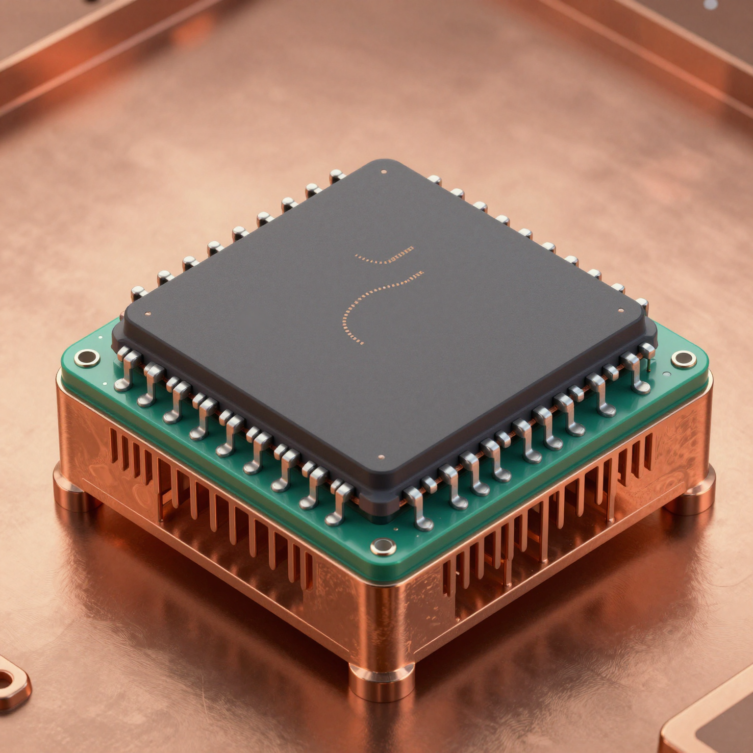
Packaging
BGAs are increasingly common in high-performance ICs, offering superior thermal and electrical performance compared to traditional leaded packages. However, BGA assembly presents unique challenges due to hidden solder joints beneath the chip.
Proper PCB assembly for electronics involving BGAs demands strict process control, X-ray inspection, and optimized reflow profiles. Misalignment or voids in solder joints can lead to intermittent failures or complete malfunction. For insights into overcoming these issues, see our detailed post on BGA assembly challenges.
Flexible and Rigid-Flex PCBs
Flexible circuits enable innovative form factors in wearable tech, foldable displays, and medical devices. Assembling flexible PCBs requires specialized handling, fixtures, and soldering techniques to prevent damage during PCB assembly for electronics.
Designers must also consider dynamic bending, material compatibility, and adhesion when planning flexible PCB layouts. Best practices include avoiding stiffeners near bend zones and ensuring proper via placement. Explore our guide on flexible PCB design best practices for actionable tips.
Quality Control in PCB Assembly for Electronics
No discussion of PCB assembly for electronics would be complete without addressing quality assurance. Defects introduced during assembly—such as cold solder joints, tombstoning, bridging, or misaligned components—can compromise device functionality and longevity.
A comprehensive quality control strategy includes multiple inspection stages throughout the PCB assembly for electronics process:
Automated Optical Inspection (AOI)
AOI systems use high-resolution cameras and image processing software to detect defects after solder paste application and component placement. They identify missing components, incorrect polarity, skew, and solder bridging with remarkable speed and accuracy.
X-Ray Inspection (AXI)
For components with hidden solder joints—like BGAs and quad flat no-leads (QFNs)—X-ray inspection is indispensable. AXI reveals internal structures, enabling detection of voids, insufficient solder, and alignment issues not visible to the naked eye or AOI.
In-Circuit Testing (ICT) and Functional Testing
After assembly, boards undergo electrical testing to verify connectivity, resistance, capacitance, and signal integrity. ICT checks individual components, while functional testing simulates real-world operation to confirm overall performance.
Implementing a structured approach ensures consistent results. Our 6-step quality control process outlines best practices for minimizing defects and maximizing yield.
Choosing the Right Partner for PCB Assembly for Electronics
Outsourcing PCB assembly for electronics to a capable manufacturer can significantly reduce time-to-market, improve quality, and lower costs. When evaluating potential partners, consider the following criteria:
- Technical Capabilities: Can they handle your required technologies (e.g., SMT, THT, HDI, BGA)?
- Component Sourcing: Do they offer reliable electronic component sourcing and supply chain management?
- Quality Certifications: Are they ISO-certified? Do they follow IPC standards?
- Turnaround Time: How quickly can they prototype and scale production?
- Support Services: Do they provide DFM analysis, testing, and after-sales support?
One trusted provider offering end-to-end solutions is a professional PCB assembly manufacturer, which supports everything from prototyping to high-volume production across industries like healthcare, telecommunications, and IoT.
Their capabilities include advanced SMT lines, automated optical and X-ray inspection, and rigorous QA protocols tailored to meet diverse industry needs. Whether you're developing a simple control board or a complex RF module, partnering with an experienced team ensures your PCB assembly for electronics meets the highest standards.
Emerging Trends in PCB Assembly for Electronics
The landscape of PCB assembly for electronics continues to evolve with technological advancements and market demands.
Miniaturization and Increased Integration
Devices are getting smaller while packing more features. This trend pushes PCB assembly for electronics toward finer pitch components, embedded passives, and 3D packaging solutions. Manufacturers must invest in ultra-precision equipment and cleanroom environments to maintain yields.
Sustainability and Lead-Free Processes
Environmental regulations like RoHS (Restriction of Hazardous Substances) mandate lead-free solders and eco-friendly materials. While beneficial for sustainability, lead-free assembly requires higher reflow temperatures and careful process tuning to avoid defects.
Smart Manufacturing and Industry 4.0
Digital transformation is reshaping PCB assembly for electronics through smart factories equipped with IoT sensors, predictive maintenance, and real-time data analytics. These tools enhance traceability, reduce downtime, and improve decision-making across the production line.
For example, digital twin technology allows manufacturers to simulate assembly processes before physical production begins, identifying potential issues early. Similarly, AI-driven optical inspection systems improve defect recognition over time through machine learning.
Supply Chain Resilience
Recent global disruptions have highlighted vulnerabilities in the electronics supply chain. Forward-thinking companies now prioritize dual sourcing, inventory buffering, and localized manufacturing to mitigate risks. Optimizing the PCB supply chain ensures continuity and responsiveness in PCB assembly for electronics operations.
Learn more about strategies in our article on PCB supply chain optimization.
Conclusion: The Critical Role of PCB Assembly for Electronics
PCB assembly for electronics is far more than a manufacturing step—it's the bridge between design intent and real-world functionality. As electronic systems grow in complexity and performance demands rise, the importance of precision, reliability, and innovation in assembly cannot be overstated.
From selecting the appropriate technology (SMT, THT, or hybrid) to implementing robust quality controls and embracing emerging trends, success in PCB assembly for electronics hinges on expertise, infrastructure, and strategic partnerships.
Whether you're launching a new product or scaling existing production, investing in a knowledgeable and capable manufacturing partner ensures your electronics perform reliably in the hands of users. For those seeking expert guidance, exploring resources like the complete guide to PCB assembly or reaching out to a reputable contact PCB manufacturer can provide valuable support.
As we move into an era defined by AI, 5G, autonomous systems, and connected devices, PCB assembly for electronics will remain at the heart of technological progress—powering the innovations that shape our future.