Complete Guide to PCB Assembly Process: From Design to Production with SUNTOP Electronics
Amos-the Electronics engineer
In today’s rapidly evolving electronics landscape, printed circuit boards (PCBs) are the backbone of virtually every modern device — from smartphones and medical equipment to industrial automation systems and automotive electronics. Behind every reliable electronic product lies a complex and meticulously executed PCB Assembly Process, transforming a bare circuit board into a fully functional component ready for integration.
At SUNTOP Electronics, we pride ourselves on being more than just a PCB assembly manufacturer — we are your end-to-end partner in innovation, offering comprehensive PCB assembly services that span from initial design support through final production and quality assurance. Whether you're developing a prototype or scaling up for mass production, understanding the full scope of the PCB Assembly Process is essential to ensuring performance, reliability, and cost-efficiency.
This guide will walk you through every stage of the PCB Assembly Process, highlighting best practices, technological advancements, and how SUNTOP Electronics ensures excellence at each step — all under the umbrella of our seamless From Design to Production workflow.
What Is PCB Assembly?
Before diving into the process, it's important to define what PCB assembly actually means. While often confused with PCB fabrication, PCB assembly refers specifically to the process of mounting and soldering electronic components onto a fabricated bare PCB. This transforms the board from a passive substrate into an active, functional unit — commonly referred to as a PCBA (Printed Circuit Board Assembly).
The PCB Assembly Process involves several critical stages:
- Design validation
- Component sourcing
- Solder paste application
- Component placement
- Reflow soldering
- Inspection and testing
Each phase demands precision engineering, advanced machinery, and rigorous quality control — areas where SUNTOP Electronics excels as a leading provider of PCB assembly services.
The Importance of a Seamless From Design to Production Workflow
Developing a successful electronic product isn’t just about creating a great schematic; it requires a holistic approach that integrates design, manufacturability, supply chain logistics, and scalability. That’s why SUNTOP emphasizes a unified From Design to Production strategy.
A fragmented workflow — where design teams work independently from manufacturing partners — can lead to costly delays, redesigns, and yield issues. By contrast, collaborating early with an experienced PCB assembly manufacturer like SUNTOP ensures:
- Design for Manufacturability (DFM) checks are performed upfront
- Component availability and lifecycle status are verified
- Assembly methods are optimized for efficiency and reliability
- Prototyping timelines are reduced
- Time-to-market is accelerated
Our engineers work closely with clients during the pre-production phase to review Gerber files, BOMs (Bill of Materials), and assembly drawings, identifying potential risks before any physical production begins.
Step-by-Step Breakdown of the PCB Assembly Process
Let’s now explore the detailed steps involved in the modern PCB Assembly Process, using SUNTOP Electronics’ industry-leading methodologies as a benchmark.
1. Design Review and DFM Analysis
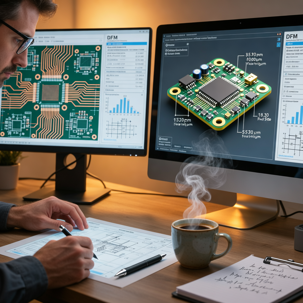
Every successful assembly starts with a solid design. At SUNTOP, the first technical step after receiving client data is a comprehensive Design for Manufacturability (DFM) analysis.
We examine:
- Trace widths and spacing
- Pad sizes and via placements
- Component footprints
- Thermal relief considerations
- Layer stack-up compatibility
Using advanced software tools, we simulate how the board will behave during soldering, reflow, and mechanical stress. Any discrepancies between the intended design and practical manufacturability are flagged and discussed with the customer.
This proactive review prevents common pitfalls such as tombstoning, bridging, or misalignment during automated assembly — saving time, materials, and costs downstream.
🔍 Pro Tip: Always provide your manufacturer with complete design packages including Gerber files, NC drill files, BOM, and assembly drawings to streamline this process.
For more insights on optimizing your designs, check out our article on flexible PCB design best practices.
2. Bare PCB Fabrication
While technically part of PCB fabrication rather than assembly, the quality of the base board directly impacts the success of the entire PCB Assembly Process. SUNTOP offers integrated PCB manufacturing services, allowing us to maintain strict control over material selection, impedance control, surface finishes, and dimensional accuracy.
Key factors include:
- Substrate Material: FR-4, Rogers, polyimide, etc., selected based on thermal, electrical, and mechanical requirements.
- Copper Weight: Ranges from 0.5 oz to 4+ oz depending on current-carrying needs.
- Surface Finish: Options like ENIG, HASL, Immersion Silver, or OSP ensure good solderability and shelf life.
Our PCB manufacturing capabilities include HDI, rigid-flex, and high-frequency RF boards — enabling support for cutting-edge applications across aerospace, telecommunications, and medical devices.
For deeper insight into surface finish options, read our detailed PCB surface finishes guide.
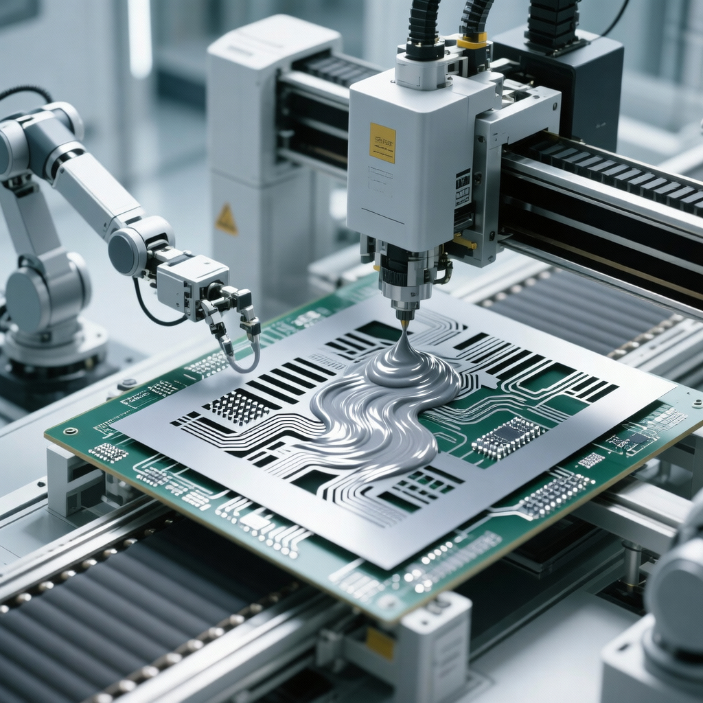
3. Solder Paste Application
Once the bare PCBs pass incoming inspection, the next step is applying solder paste — a sticky mixture of tiny solder particles and flux that temporarily holds components in place before permanent soldering.
This is done using a stencil printer:
- A stainless steel stencil, laser-cut to match pad locations, is aligned precisely over the PCB.
- Solder paste is spread across the stencil using a squeegee.
- As the stencil is lifted, precise deposits remain on the pads.
Accuracy here is crucial — too much paste causes bridging; too little leads to weak joints. SUNTOP uses automated vision systems to verify alignment and consistency after each print cycle.
Common solder pastes used:
- Type 3, Type 4, or Type 5 (particle size varies)
- Lead-free (e.g., SAC305) or leaded formulations based on RoHS compliance needs
4. Component Placement (Pick-and-Place)
After solder paste application comes one of the most dynamic phases: component placement. Modern assemblies rely heavily on Surface Mount Technology (SMT), where components are placed directly onto the surface of the board.
Using high-speed pick-and-place machines, components are retrieved from reels, trays, or tubes and positioned with micron-level accuracy. These machines use vacuum nozzles and optical recognition systems to align parts correctly.
Types of components handled:
- Resistors, capacitors (0201, 0402, 0603 packages)
- ICs (QFP, QFN, BGA)
- Connectors and discrete semiconductors
Through-hole components may still be used in certain designs, especially for high-power or mechanical strength requirements. For a comparison of these two methods, see our in-depth article on SMT vs through-hole assembly.
At SUNTOP, our SMT lines operate at speeds exceeding 80,000 components per hour while maintaining ±25µm placement accuracy — ideal for dense, high-complexity boards.
5. Reflow Soldering
With components seated in the solder paste, the board enters the reflow oven — a multi-zone conveyor furnace that gradually heats the PCB to melt the solder and form reliable electrical and mechanical connections.
The reflow profile typically includes four stages:
- Preheat: Gradual temperature rise to activate flux and prevent thermal shock.
- Thermal Soak: Evens out temperature across the board and activates flux to clean oxides.
- Reflow/Peak: Temperature exceeds solder melting point (typically ~217°C for SAC305), forming intermetallic bonds.
- Cooling: Controlled cooling solidifies the joints and ensures structural integrity.
Improper profiles can cause defects like voiding, balling, or delamination. SUNTOP employs real-time thermocouples and statistical process control (SPC) to monitor and optimize every run.
For high-reliability sectors like automotive or defense, we also offer nitrogen-reflow environments to reduce oxidation and improve joint quality.
6. Through-Hole Component Insertion and Wave Soldering
If the design includes through-hole components (THT), these are inserted either manually or via automated insertion machines after SMT processing.
These boards then go through wave soldering:
- The bottom side of the PCB passes over a standing wave of molten solder.
- Capillary action draws the solder up through the holes, forming strong mechanical and electrical connections.
Selective soldering techniques are used when only specific areas need THT treatment, avoiding damage to already-assembled SMDs.
Post-solder cleaning may follow if required by application standards (e.g., medical or military specs).
7. Manual Assembly and Rework
Despite automation, some tasks require human expertise. Skilled technicians perform:
- Hand soldering of large connectors or heat-sensitive components
- Rework of defective joints identified during inspection
- Conformal coating application
- Potting or encapsulation
SUNTOP’s trained operators adhere to IPC-A-610 Class 2 or Class 3 standards, ensuring consistent quality even in manual operations.
Rework stations are equipped with microscopes, hot-air rework tools, and desoldering pumps to correct issues without damaging surrounding circuitry.
8. Automated Optical Inspection (AOI)
Quality assurance begins immediately after soldering. Automated Optical Inspection (AOI) systems scan the board using high-resolution cameras and sophisticated algorithms to detect defects such as:
- Missing components
- Misaligned or rotated parts
- Solder bridges
- Insufficient or excessive solder
- Polarity errors
AOI is non-destructive and fast — capable of inspecting thousands of solder joints per minute. Results are logged for traceability and trend analysis.
At SUNTOP, AOI is deployed both post-SMT and post-THT to catch issues early and minimize scrap rates.
9. X-Ray Inspection (AXI) for Hidden Joints
Some components, particularly Ball Grid Arrays (BGAs) and Chip Scale Packages (CSPs), have solder joints hidden beneath the body. Visual inspection cannot assess their quality.
That’s where X-ray inspection (AXI) becomes indispensable. Using X-rays to penetrate the package, AXI reveals:
- Void percentage in solder balls
- Alignment of balls with pads
- Presence of shorts or opens
- Head-in-pillow defects
SUNTOP utilizes state-of-the-art AXI systems with 2D and 3D imaging capabilities to ensure BGAs meet stringent reliability standards.
Understanding BGA assembly challenges is key to preventing field failures — especially in mission-critical applications.
10. Functional Testing and In-Circuit Testing (ICT)
Even visually perfect boards may have underlying electrical faults. To confirm functionality, we perform various electrical tests:
In-Circuit Testing (ICT)
- Uses a bed-of-nails fixture to make contact with test points.
- Measures resistance, capacitance, voltage levels, and continuity.
- Detects shorts, opens, wrong values, and orientation errors.
ICT provides deep diagnostics but requires custom tooling, making it more suitable for medium to high-volume runs.
Flying Probe Testing
- Ideal for low-volume or prototype batches.
- Probes move dynamically across the board without a fixed fixture.
- Slower than ICT but highly flexible.
Functional Circuit Testing (FCT)
- Simulates real-world operating conditions.
- Powers up the board and verifies input/output signals, communication interfaces, power regulation, etc.
- Often customized per project with dedicated test jigs and software.
At SUNTOP, we develop tailored test strategies based on volume, complexity, and application risk level.
11. Final Cleaning, Coating, and Packaging
Depending on the end-use environment, additional finishing steps may be applied:
Conformal Coating
- A protective polymer layer (acrylic, silicone, urethane) applied to guard against moisture, dust, chemicals, and thermal cycling.
- Applied via spraying, dipping, or selective coating robots.
Used extensively in automotive, outdoor, and industrial controls.
Potting
- Encapsulating the entire assembly in resin for extreme protection.
- Common in high-vibration or submersible devices.
Final Cleaning
- Removes flux residues, especially important in high-impedance circuits.
- Deionized water or solvent-based cleaning processes used.
Boards are then dried, labeled, and packed in ESD-safe packaging for shipment.
12. Quality Assurance and Traceability
At SUNTOP Electronics, quality isn't an afterthought — it's embedded into every phase of the PCB Assembly Process. Our 6-step quality control process ensures zero-defect delivery:
- Incoming Material Inspection
- Solder Paste Verification
- Pre-Reflow AOI
- Post-Reflow AOI
- AXI (for BGAs/CSPs)
- Final Electrical & Functional Test
All inspections are documented, and lot traceability is maintained throughout production. We comply with ISO 9001, IATF 16949 (automotive), and IPC standards.
Our QA services include environmental stress screening (ESS), HALT/HASS testing, and first-article reporting upon request.
Types of PCB Assembly Technologies
The choice of assembly technology depends on design complexity, component types, and production volume. Here are the primary methods used today:
Surface Mount Technology (SMT)
- Components mounted directly onto the surface of the PCB.
- Enables smaller, lighter, and denser designs.
- Dominates >80% of modern electronics.
Ideal for consumer electronics, IoT devices, and mobile tech.
Through-Hole Technology (THT)
- Leads inserted through drilled holes and soldered on the opposite side.
- Offers superior mechanical strength and durability.
- Used for connectors, transformers, and heavy-duty components.
Still relevant in power electronics, military/aerospace, and industrial machinery.
Mixed-Technology Assembly
- Combines both SMT and THT on the same board.
- Requires careful sequencing to avoid disturbing previously assembled parts.
Common in hybrid products like power supplies and control panels.
SUNTOP supports all three approaches with flexible line configurations and expert process planning.
Advanced PCB Assembly Challenges and Solutions
As electronics shrink and performance demands grow, new challenges emerge in the PCB Assembly Process. Let’s look at some of the most pressing ones and how SUNTOP addresses them.
Miniaturization and High-Density Interconnect (HDI)
Modern devices demand smaller footprints and higher functionality. HDI PCBs use microvias, blind/buried vias, and finer pitch components (e.g., 0.3mm pitch BGAs).
Challenges:
- Tight tolerances require ultra-precise placement
- Microvia reliability under thermal cycling
- Increased risk of solder voiding
Solutions at SUNTOP:
- Use of advanced pick-and-place machines with enhanced vision systems
- Optimized reflow profiles with nitrogen atmosphere
- Enhanced X-ray inspection for micro-BGAs
Learn more about the future of miniaturization in our article on HDI PCB technology.
Lead-Free Soldering Compliance
Environmental regulations like RoHS mandate the use of lead-free solders (e.g., SAC305), which have higher melting points (~217°C) compared to traditional SnPb (~183°C).
Impact:
- Greater thermal stress on components and substrates
- Risk of pad cratering or delamination
- More sensitive reflow profiling needed
Our engineers use predictive modeling and thermal simulation to optimize profiles, minimizing stress while ensuring robust joints.
Supply Chain Volatility and Component Sourcing
One of the biggest hurdles in recent years has been semiconductor shortages and long lead times. Delays in obtaining key components can stall entire projects.
SUNTOP mitigates this through our electronic component sourcing services:
- Strategic partnerships with global distributors
- Lifecycle monitoring and obsolescence alerts
- Approved alternatives database (with customer approval)
- Dual-sourcing strategies
We help clients navigate disruptions and keep production on track — even during market turbulence.
Read our latest insights on PCB supply chain optimization to learn how we’re building resilient supply chains.
Why Choose SUNTOP Electronics for Your PCB Assembly Needs?
With numerous PCB assembly manufacturers available globally, what sets SUNTOP apart?
End-to-End Capabilities
From concept to completion, we offer:
- PCB design support
- Fabrication and assembly
- Component procurement
- Testing and certification
- Logistics and fulfillment
No need to coordinate multiple vendors — we manage it all.
State-of-the-Art Facilities
Our manufacturing floor features:
- Fully automated SMT lines with SIPLACE and Yamaha machines
- Nitrogen reflow ovens with real-time profiling
- 3D AOI and AXI systems
- Environmental testing chambers
All housed in an ESD-controlled, cleanroom environment.
Industry-Specific Expertise
We serve diverse markets, including:
- Medical devices
- Automotive and EV systems
- Industrial automation
- Telecommunications
- Consumer electronics
- Aerospace and defense
Each sector has unique regulatory and reliability demands — and SUNTOP meets them all.
Explore the industries served by PCB manufacturer to see how we tailor solutions to your field.
Commitment to Transparency and Support
We believe in open communication. Clients receive:
- Real-time production updates
- Detailed inspection reports
- First-article samples
- Dedicated project managers
Plus, our team is always available to answer questions or assist with design improvements.
Want to learn more about who we are? Visit our about PCB assembly company page.
How to Get Started with SUNTOP’s PCB Assembly Service
Beginning a new project should be exciting, not overwhelming. Here’s how easy it is to start working with SUNTOP:
-
Submit Your Files
- Send Gerber files, BOM, and assembly drawings via email or our secure upload portal.
-
Receive a Free DFM Report
- Within 24–48 hours, get actionable feedback on design readiness.
-
Get a Quote
- Transparent pricing based on volume, complexity, and turnaround time.
-
Approve and Launch Production
- Once approved, we begin fabrication and assembly with regular progress updates.
To begin, simply contact PCB manufacturer or click get a PCB quote for immediate assistance.
Our responsive team is ready to help whether you’re building a single prototype or launching a global product line.
Conclusion: Mastering the PCB Assembly Process from Design to Production
The journey from a circuit diagram to a fully assembled, tested, and certified PCB is intricate — requiring technical mastery, advanced equipment, and unwavering attention to detail. The PCB Assembly Process is not merely a sequence of steps; it’s a symphony of precision engineering, material science, and quality assurance.
At SUNTOP Electronics, we’ve refined this process over years of delivering high-reliability assemblies across industries. Our commitment to excellence, transparency, and partnership makes us a preferred choice for innovators worldwide.
Whether you're navigating the complexities of HDI boards, managing supply chain risks, or preparing for mass production, our PCB assembly services provide the foundation you need to succeed.
By integrating design, fabrication, assembly, and testing under one roof, we deliver true From Design to Production continuity — reducing risk, improving speed, and enhancing product quality.
Ready to bring your next idea to life? Partner with SUNTOP Electronics — your trusted ally in electronic manufacturing innovation.