Printed Circuit Board Manufacturing Process: Key Steps, DFM Risks, and What to Send for Quote
SUNTOP Electronics
Printed circuit board manufacturing is the process of turning design data into bare boards that can be fabricated consistently, inspected clearly, and handed off to assembly with fewer surprises. For engineering and sourcing teams, the real challenge is not memorizing every factory step. It is understanding which inputs shape yield, quote speed, material choice, drill strategy, surface finish, and manufacturability before production starts. Good printed circuit board manufacturing starts with cleaner data and clearer intent, not just factory equipment.
A weak handoff package usually slows printed circuit board manufacturing long before any panel enters a production line. Missing stackup intent, unclear drill expectations, incomplete fabrication notes, and unresolved DFM questions all create back-and-forth that delays quoting and increases revision risk. A cleaner package gives the manufacturer enough context to review the board for practicality instead of guessing what the design team meant.
This article explains how the manufacturing workflow typically moves from CAM review into imaging, lamination, drilling, plating, solder mask, surface finish, inspection, and release. It also covers the common issues that create friction and what to prepare before you ask a supplier to quote or build the board.
What PCB Fabrication Includes Before Production Starts
PCB fabrication does not begin when copper is etched. It begins when the manufacturer reviews the data package and decides whether the board can be built as submitted, needs clarification, or should be adjusted before release. That front-end review often covers Gerber or ODB++ data, drill files, stackup notes, material assumptions, special process requirements, and any assembly interaction that could affect the bare board.
This early stage matters because many problems are easier to fix in engineering than on the shop floor. For example, a fabricator may need to question whether annular ring margin is realistic, whether the board outline and slots are fully defined, whether the requested finish fits the product use case, or whether the chosen material assumptions support impedance and thermal goals. A practical PCB DFM checklist helps teams catch many of those issues before files go out.
Supplier review is also where commercial and technical questions start to overlap. A sourcing manager may care about quote speed and comparability across suppliers, while an engineer may care about stackup stability, drill capability, and signal integrity. In practice, printed circuit board manufacturing review is where those priorities have to become one workable package. A strong release package supports both.
How the Workflow Moves from CAM Review to Inner-Layer Processing
Once the input package is accepted, the board moves into process preparation. CAM engineers verify layer data, map drill programs, review copper balance, and confirm that the board structure matches the requested build intent. If the board is multilayer, inner layers are prepared before lamination, which means imaging and etching work begins with the copper pattern that will later be buried inside the finished stack. This is the point where printed circuit board manufacturing stops being a drawing exercise and becomes a controlled production workflow.
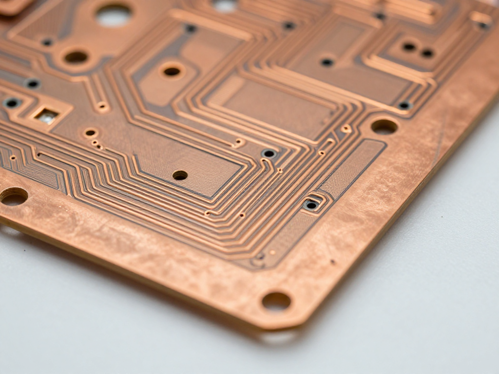
This close-up highlights the kind of copper pattern definition and hole detail that manufacturers review before multilayer fabrication moves deeper into the process.
At a high level, this part of the workflow usually includes:
- data normalization and panel planning
- inner-layer imaging and etching
- oxide or surface preparation before lamination
- layer registration and lamination setup
- post-lamination drilling and hole-wall preparation
The exact workflow varies by board type, but the principle stays the same: the manufacturer is translating digital intent into a stable physical structure. That is why details such as layer count, copper weight assumptions, dielectric selection, and drill structure need to be coherent before release. Even common materials such as FR-4 involve tradeoffs around electrical performance, thickness control, and downstream processing.
For teams comparing suppliers, printed circuit board manufacturing quality is influenced as much by process discipline as by nominal capability lists. A factory that asks clarifying questions early is often reducing later risk, not creating unnecessary friction. If your project includes controlled impedance, specialty laminates, or tight fabrication constraints, supplier capability review is worth doing before quoting.
Drilling, Plating, Solder Mask, and Surface Finish Choices That Affect Yield
After lamination, printed circuit board manufacturing becomes highly sensitive to drill quality, plating consistency, registration control, solder mask definition, and finish selection. These are not isolated steps. They interact with the design choices already locked into the board.
Drilling must match the real structure of the board. Hole size, aspect ratio, via count, and positional tolerance expectations affect both manufacturability and reliability. If the drill strategy is too aggressive for the stackup, yield risk can rise quickly. After drilling, plated-through-hole quality matters because copper deposition inside the hole walls is part of the electrical structure, not just a cosmetic detail.
Solder mask is another area where fabrication decisions influence downstream assembly results. Mask clearance, pad definition, and registration all affect how cleanly the board can move into PCBA. Surface finish selection then adds another layer of tradeoff. ENIG, HASL, immersion silver, immersion tin, and OSP each bring different considerations for flatness, shelf life, corrosion exposure, and assembly compatibility. Our surface finishes guide is a useful follow-on reference when teams need to compare those options more closely.
During this stage, process control also depends on inspection discipline. Automated optical inspection, electrical testing strategy, and final visual checks help confirm that the delivered board matches the released data instead of only looking acceptable at a glance. Industry references such as IPC matter here because they provide a common language for acceptability and communication, even though each project still needs its own engineering judgment.
Common Fabrication Risks That Slow Quotes or Create Rework
Most printed circuit board manufacturing delays come from preventable ambiguity rather than dramatic factory failure. One common problem is incomplete fabrication documentation. If the design files do not make it clear which material family, finish, thickness target, or stackup intent matters, the supplier has to pause and ask for clarification.
Another problem is treating CAD output as if it were a complete manufacturing package. A board may pass internal design checks and still create fabrication issues because drill notes are incomplete, impedance intent is undocumented, slots are inconsistently defined, or mechanical and copper data do not fully agree.
A third risk is late discovery of assembly interaction. Bare-board decisions influence assembly yield, especially around pad definition, mask strategy, panelization, fiducials, and warpage risk. When those concerns stay disconnected, supplier review may finish only for the assembly team to reopen questions that could have been handled earlier.
It also creates friction when buyers compare quotes without normalizing what each supplier is actually pricing. One quote may assume a different laminate family, different finish, or different testing scope than another. The numbers look comparable, but the underlying process assumptions are not the same.
What to Send Your PCB Manufacturer Before Quote or Production
If you want better feedback and a faster path through printed circuit board manufacturing review, send a package that answers the obvious technical questions up front. In most projects that includes current fabrication files, drill data, board outline information, layer count and stackup intent, finished thickness target when known, surface finish expectation, and notes about anything still open to supplier recommendation.
It also helps to explain the project context in one short paragraph. Is the board an early prototype, a pilot build, or a production transfer? Are impedance targets fixed? Is the team open to stackup alternatives? Does the board need a bare-board-only quote or coordinated PCBA review as well? Good answers improve the quality of printed circuit board manufacturing feedback because the supplier can focus on the real decision points.
If assembly will follow quickly, include the information that helps bridge fabrication and PCBA expectations rather than treating them as separate worlds. Teams that need combined support can use the contact page to share files and request an engineering review before final release.
A practical pre-quote package usually includes:
- fabrication data and drill files matching the current revision
- stackup notes or material expectations when known
- board outline, slots, cutouts, and special mechanical features
- finish preference or acceptable finish options
- quantity stage context such as prototype or production intent
- any known risk areas where supplier feedback is specifically requested
FAQ About PCB Fabrication Review
What is the difference between PCB fabrication and PCB assembly?
PCB fabrication refers to building the bare board structure itself, including layer processing, drilling, plating, solder mask, finish, and inspection. PCB assembly happens after that, when components are mounted and soldered onto the finished board.
When should a team involve a supplier in printed circuit board manufacturing review?
As early as the team has a stable enough layout and stackup direction to discuss real constraints. Early review is especially useful when the board includes controlled impedance, dense drilling, unusual materials, or handoff uncertainty between fabrication and assembly.
Does every project need a detailed fabrication note package?
Not every board needs an unusually long document, but every project benefits from clear and consistent manufacturing intent. The more complex the board, the more valuable explicit notes become.
What usually causes the biggest delay in PCB manufacturing quotes?
The most common cause is missing or ambiguous information. When the supplier has to infer stackup, finish, drill expectations, or revision status, quote turnaround slows and technical risk rises.
Conclusion
Good printed circuit board manufacturing depends on clearer inputs, not just better machines. When teams define the board structure, document open questions, and connect fabrication choices to assembly and product goals, they reduce avoidable back-and-forth and improve quote quality. Strong printed circuit board manufacturing results usually come from early alignment, disciplined review, and a release package that makes supplier decisions easier.
The best handoff is usually the one that makes engineering intent easy to review. If your team wants a second set of eyes on stackup assumptions, fabrication notes, or manufacturability risk before release, it is worth involving the manufacturing partner early instead of waiting for problems to surface after the quote cycle has already started.