Embedded Components PCB Guide: Design Tradeoffs, Manufacturing Constraints, and When It Fits
SUNTOP Electronics
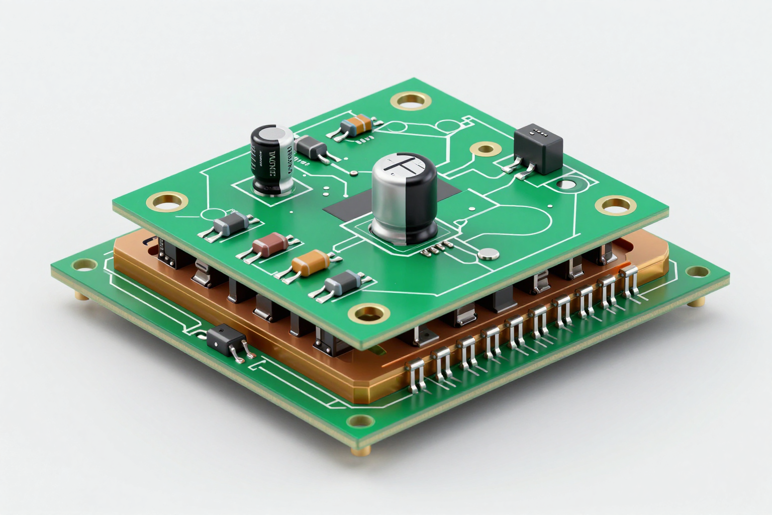
An embedded components PCB places selected parts inside the board structure instead of mounting every component only on the outer surfaces. In most projects, that means embedding passives such as resistors or capacitors between layers, although some advanced programs also explore more specialized structures.
Teams usually look at an embedded components PCB when board area is tight, electrical paths need to stay short, or product architecture is pushing conventional placement limits. The concept can be valuable, but it should not be treated as a fashionable shortcut. This buried-component approach changes fabrication flow, inspection access, rework options, and the way a manufacturing partner reviews risk.
That is why the right first question is not whether the concept sounds advanced. The better question is whether the product has enough density, performance, or packaging pressure to justify the added process complexity. For many products, a cleaner multilayer layout or a smarter assembly strategy will solve the problem at lower risk.
This guide explains where an embedded components PCB makes sense, what technical limits should be reviewed early, and how to frame the conversation with a PCB/PCBA manufacturing partner before design decisions get locked in.
What an Embedded Components PCB Means and Why Teams Consider It
An embedded components PCB is part of a broader miniaturization and integration approach. Instead of placing every passive on the board surface, some components are buried into internal layers so routing, top-side real estate, or assembly density can be managed differently.
The main attraction is not novelty. It is system packaging efficiency. Teams may consider this route when:
- board outline is fixed but function count keeps growing
- signal or power paths benefit from shorter interconnect distance
- dense modules need more free surface area for active devices or connectors
- a product is space-constrained enough that conventional assembly options are becoming awkward
In practice, this approach often appears next to HDI thinking, sequential lamination decisions, or other advanced stackup questions. That is why it helps to compare the concept with a more standard multilayer PCB design approach before assuming the buried route is necessary. It is also worth remembering that the larger discipline still sits inside design for manufacturability, not outside it.
Which Components Are Commonly Embedded and What Benefits Teams Expect
Most programs discussing an embedded components PCB start with passives, not with highly complex active packages. Embedded resistors and capacitors are easier to justify because they can support density goals without forcing the full manufacturing and thermal burden that more complicated embedded structures might introduce.
The expected benefits usually include:
- more outer-layer area for ICs, connectors, shielding, or test access
- shorter electrical paths in selected networks
- cleaner module integration in compact products
- fewer surface-mounted parts in zones where placement competition is severe
Those benefits are real only when the product architecture actually needs them. This approach is not automatically cheaper, easier to source, or faster to industrialize. Once components are buried, every stackup choice becomes more coupled to the manufacturing process. Material selection, lamination sequence, via planning, and test strategy all need more discipline.
For RF, high-speed, or dense industrial electronics, teams may also need to align the buried-component concept with dielectric and signal-integrity choices. That is where adjacent topics such as high frequency PCB materials and high-density interconnect become relevant reference points rather than separate conversations.
Layout, Stackup, and Manufacturing Constraints to Evaluate Early
This kind of board should be reviewed as a fabrication structure first and a layout trick second. If the buried elements are added late, the board can become difficult to quote and even harder to build consistently.
Start with stackup ownership
The stackup cannot stay generic. An embedded components PCB needs clear decisions on cavity strategy or embed layer position, lamination sequence, dielectric build, copper distribution, and via interaction. Even when the exact process is supplier-specific, design teams should still define the board intent well enough for a manufacturer to evaluate feasibility.
Check manufacturability around the buried parts
Review whether the buried-component structure creates local thickness changes, copper imbalance, fragile routing windows, or drill interactions that become difficult after lamination. Buried parts can influence resin flow, registration, and later process stability. If those consequences are only discovered during quote review, the project usually loses time.
Keep documentation explicit
The release package for an embedded components PCB should state what is embedded, where it sits in the structure, and what process assumptions matter. A supplier should not have to infer buried-component intent from partial drawings or from CAD layer names alone. If your team wants an early feasibility discussion, the safest route is to brief the manufacturer through a structured capabilities review before freezing the stackup.
Inspection, Assembly, and Rework Tradeoffs Teams Often Underestimate
The biggest hidden cost is often not the initial concept work. It is the loss of access after the board is built. Once a component is inside the structure, direct visual inspection and post-build replacement options change dramatically.
Inspection strategy therefore matters early. This kind of design may need more emphasis on process control, incoming material confidence, electrical verification, and cross-section learning during development. Teams should not assume that buried parts can be checked in the same way as ordinary surface-mounted passives.
Rework is another major issue. A surface resistor that fails review can often be replaced. A resistor buried inside an embedded components PCB usually cannot. That means component quality, design margin, and manufacturing discipline become more important before release, not after pilot builds.
Assembly planning still matters too. Even if some passives are embedded, the rest of the board may remain a complex PCBA with connectors, BGAs, shielding, or mixed-technology assembly. The buried approach should reduce a real packaging problem, not create an exotic structure that complicates the full product without enough return.
How to Brief a PCB Manufacturing Partner on an Embedded Components PCB Project
A productive supplier discussion starts with clarity. If you want useful feedback on this concept, send more than Gerbers and a general note that some parts are internal.
A cleaner briefing package should include:
- the product reason for considering the buried-component structure
- the target embedded component types and approximate locations
- stackup intent and any nonstandard lamination assumptions
- key electrical or packaging constraints driving the concept
- inspection or qualification concerns already identified by the design team
- questions where you want the manufacturer to challenge the approach early
This is also a good stage to ask whether a conventional architecture could achieve the same goal with less risk. Sometimes the best outcome of the review is confirmation that the buried approach is justified. Other times, the better outcome is learning that a more standard board plus assembly optimization will be easier to launch and maintain.
If your team is comparing options or preparing an RFQ, a short technical discussion through the contact page can prevent weeks of back-and-forth later.
FAQ About Embedded Components PCB
Is an embedded components PCB always smaller than a conventional board?
Not always. This approach can free surface area or help package density, but total board thickness, process margin, and surrounding layout rules may offset some of that gain.
Is an embedded components PCB suitable for every production program?
No. An embedded components PCB is usually best reserved for products with real packaging, electrical, or integration pressure. If the design goal can be met with a cleaner standard layout, that path is often easier to source, inspect, and maintain.
When should a manufacturer be involved?
Early. An embedded components PCB should be discussed before stackup and documentation are frozen, because feasibility, inspection strategy, and process risk all depend on supplier-specific manufacturing reality.
An embedded components PCB can be a strong engineering choice when miniaturization pressure is real and the project team understands the manufacturing consequences. The value comes from solving a concrete packaging problem, not from using a more advanced structure for its own sake. If the concept is on your roadmap, review it with manufacturing constraints in mind before release, not after the board package is already committed.