Multilayer PCB Design Guide: Stackup Planning, Layer Count, and Manufacturing Tradeoffs
SUNTOP Electronics
Multilayer PCB design is not just about adding more copper layers when a board starts to feel crowded. In real projects, multilayer PCB design is the process of balancing routing density, signal integrity, power distribution, mechanical limits, assembly practicality, and cost before files ever reach fabrication.
A simple two-layer board can work well for many products, but once a design needs tighter routing, cleaner return paths, controlled impedance, denser component escape, or better EMI behavior, multilayer PCB design becomes the more realistic path. The question is not whether more layers look advanced. The question is whether those layers solve a real electrical or manufacturing problem.
That is why good multilayer PCB design starts early. Teams that wait until the end of layout to decide layer count usually create avoidable rework: power planes get compromised, stackup intent stays vague, and the manufacturer has to clarify basic assumptions before quoting. A better approach is to decide what the board needs to do, then shape the layer structure around those requirements.
This guide explains where a multilayer board strategy creates value, how to think about stackup and reference planes, what manufacturability tradeoffs show up around vias and escapes, and what to include before asking a supplier to review the board.
What Multilayer PCB Design Means and When Extra Layers Are Worth It
Multilayer PCB design usually refers to a board built with three or more conductive layers laminated into one structure, although many practical projects start with four-layer, six-layer, or eight-layer decisions. The main reason to choose multilayer PCB design is not fashion. It is to create enough room for signals, planes, and component breakouts without forcing weak compromises into the layout.
In practice, extra layers are often justified when a board needs:
- dedicated reference planes for cleaner return current paths
- better separation between noisy and sensitive routing
- controlled impedance planning for high-speed or RF nets
- more stable power distribution across multiple rails
- denser BGA or fine-pitch escape routing
- less congestion around connectors, memory, processors, or mixed-signal zones
Multilayer PCB design can also improve overall board size efficiency. Instead of stretching the outline larger to make routing fit on fewer layers, a team may keep the board more compact by moving part of the complexity into the stackup. That can help enclosure fit and cable management, but it also increases fabrication complexity, so the tradeoff needs to be intentional.
The key point is that multilayer PCB design should be driven by electrical and manufacturing needs, not by a vague assumption that “more layers are always better.” If the design can stay simple without sacrificing performance or reliability, fewer layers may still be the better business decision.
How to Plan Stackup, Signal Layers, and Reference Planes
The heart of multilayer PCB design is stackup planning. Once a layer count is chosen, the next step is deciding what each layer is expected to do and how nearby layers support that purpose. Strong multilayer PCB design usually gives every important signal layer a clear reference plane and avoids treating planes as leftover space after routing is done.
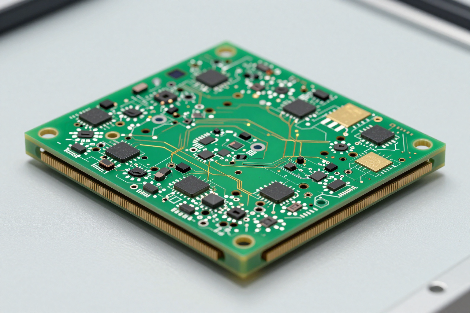
Board detail showing routed traces, via holes, and dense multilayer PCB fabrication features.
A useful starting point is to separate layer roles into a few practical buckets:
- signal layers carrying critical routing
- ground reference planes supporting return current control
- power distribution layers or copper regions
- secondary routing layers for less critical signals or breakout work
When teams skip this planning, they often end up with fragmented planes, unnecessary layer transitions, or routing that looks complete in CAD but behaves poorly in hardware. That is especially risky when the board includes fast edges, longer buses, impedance-sensitive nets, or mixed analog and digital sections.
For early feasibility work, the PCB Stackup Planner can help teams compare rough thickness, copper distribution, and layer-role assumptions before they send the design out. If specific transmission line behavior matters, the Online Impedance Calculator is a useful pre-review aid, but it should support supplier discussion rather than replace it.
Reference plane quality matters because routing behavior is strongly tied to return current paths and field structure. In broader signal integrity work, that means keeping critical traces close to a stable reference and avoiding plane breaks under those nets. If the design uses outer-layer controlled routing, common microstrip structures may be part of the stackup discussion, but the actual geometry still has to match the chosen material and fabrication process.
Good multilayer PCB design also means documenting stackup intent clearly. The fabricator should not have to guess whether a layer is meant to be a solid reference plane, whether copper balance matters in a region, or whether impedance-controlled routing is optional or mandatory.
Via Strategy, Escape Routing, and Manufacturability Tradeoffs
Via choices can make or break multilayer PCB design. A board may look routable only because the layout tool allows many layer transitions, but each transition adds cost, fabrication constraints, and possible signal or assembly side effects. Good stackup planning treats vias as a controlled resource, not an unlimited convenience.
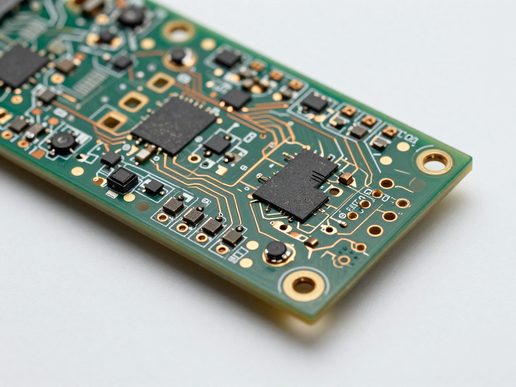
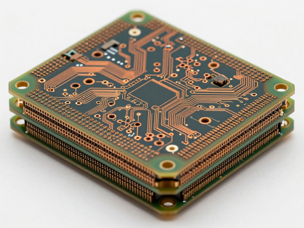
Board detail showing dense routing, component placement, and plated holes in a multilayer PCB layout.
Through vias are often the simplest and most economical option, but they consume routing channels across the full stack. Blind, buried, or microvia structures can improve density, especially around fine-pitch devices, yet they also raise process complexity and review requirements. Before using them, teams should be clear on why standard via structures are no longer enough.
Escape routing is another place where multilayer PCB design becomes a tradeoff exercise. Dense BGAs, memory interfaces, and connector fields often push designers toward higher layer counts, but the right answer is not always “add more layers immediately.” Sometimes pin swapping, component orientation changes, better fan-out planning, or a cleaner floorplan can reduce pressure before the stackup expands.
From a manufacturability view, review these items early:
- whether via structures match the actual routing need
- whether anti-pad and plane clearance assumptions are realistic
- whether high-current paths are being squeezed through narrow transitions
- whether layer changes create unnecessary return path discontinuities
- whether dense breakout areas leave enough fabrication margin
The more complex the via strategy becomes, the more important it is to discuss the design with the manufacturer before the board is treated as quote-ready.
Common Multilayer PCB Design Mistakes That Cause Cost or Delay
Most multilayer PCB design problems do not come from one dramatic failure. They come from several small decisions that interact badly once fabrication review starts.
One common mistake is choosing layer count too late. If the board is already packed and timing or power issues appear, the team may force a rushed stackup decision without enough time to reorganize routing or plane structure properly.
Another mistake is using multilayer PCB design language without real stackup definition. Saying a board is “six layers” does not tell the supplier how those layers are assigned, which nets are impedance-sensitive, or where plane continuity matters.
A third mistake is underestimating how mechanical and assembly constraints affect multilayer PCB design. Connector keepouts, stiffener needs, enclosure pressure points, component height, and test access can all change how practical a given stackup or routing choice really is.
Teams also lose time when they assume CAD design-rule checks are the same as manufacturability review. DRC may confirm that objects satisfy rule values, but it does not guarantee the release package communicates intent clearly enough for fabrication and assembly.
Finally, some boards are overbuilt. Multilayer PCB design should solve real constraints, not hide weak planning behind a higher-cost stackup. If the layer count increased only because placement, partitioning, or power strategy was never cleaned up, the quote may expose that inefficiency quickly.
How to Prepare a Better Multilayer Board Package for Manufacturing Review
The strongest stackup and routing work is only useful if the release package makes that intent easy to review. Before asking for a quote or engineering feedback, make sure the supplier can understand both the geometry and the reasoning behind the board.
A better review package usually includes:
- fabrication data and drill files that match the current revision
- stackup notes showing intended layer roles and any critical constraints
- impedance targets where they apply
- clear board outline, slots, cutouts, and mechanical notes
- assembly files if PCBA review is expected in parallel
- concise comments on what is fixed and what is still negotiable
It also helps to call out what matters most. For example, is the stackup locked because of EMC performance, or is the team open to manufacturer suggestions? Are certain layers reserved for controlled routing, or can the fabricator propose a more practical structure? Those questions affect review quality and quote speed.
If a team wants supplier input before freezing the package, the best approach is to share the design early through the contact page with a short explanation of the board objective, the current layer plan, and any known risk areas. That creates a more useful discussion than sending files with no context and waiting for issues to come back one by one.
FAQ About Multilayer PCB Design
When should a team move from two layers to multilayer PCB design?
Usually when routing congestion, reference-plane quality, power distribution, EMI control, or impedance needs cannot be solved cleanly on two layers. The move to multilayer PCB design should happen because the electrical and manufacturing case is clear, not because the board simply feels complicated.
Does multilayer PCB design always improve signal integrity?
Not automatically. Multilayer PCB design creates better options for return paths and impedance control, but only if the stackup and routing use those options correctly. A poor plane strategy on many layers can still perform worse than a disciplined simpler board.
Is a higher layer count always more expensive overall?
Bare-board fabrication cost usually rises as the stackup becomes more complex, but total project cost depends on more than fabrication alone. If multilayer PCB design reduces board area, avoids redesign, improves yield, or simplifies assembly, the broader cost picture may still improve.
What should be shared with a manufacturer before quoting a multilayer board?
Share current fabrication data, drill information, stackup intent, mechanical notes, and any constraints tied to impedance, materials, or assembly. The clearer the package is, the easier it is for a manufacturer to judge whether the multilayer PCB design is ready as-is or needs adjustment.
Conclusion
Good multilayer PCB design is a planning discipline, not just a layer-count choice. When teams define stackup roles early, protect reference planes, use vias with purpose, and communicate manufacturing intent clearly, they reduce quote friction and avoid preventable redesign loops.
The best results usually come from treating the board as a shared engineering review between layout, electrical goals, mechanical constraints, and manufacturing reality. If that alignment happens before release, the board moves forward with fewer surprises and a cleaner path to fabrication and assembly.