PCB DFM Checklist: What to Review Before You Send a Board to Manufacturing
SUNTOP Electronics
A board may look complete in CAD and still be unready for manufacturing. That gap between “design finished” and “factory-ready” is exactly where PCB DFM matters.
PCB DFM—design for manufacturability—means reviewing the board with real fabrication and assembly constraints in mind before files are released for quoting, prototyping, or volume production. It is the step where engineering intent is translated into something a PCB manufacturer and PCBA partner can build consistently, inspect reliably, and deliver without avoidable back-and-forth.
In practice, many quote delays and production issues do not come from advanced technology problems. They come from smaller misses that accumulate: unclear drill data, weak annular ring margin, incomplete stackup notes, inconsistent impedance callouts, conflicting layer naming, unrealistic solder mask spacing, missing assembly constraints, or a handoff package that leaves the manufacturer guessing.
That is why a practical PCB DFM checklist is valuable. It gives hardware teams a repeatable review structure before sending a board to fabrication or assembly. It also gives sourcing teams a better basis for comparing quotes and identifying which suppliers are truly reviewing risk versus simply pricing files as received.
This guide breaks the review into the checks that matter most before release: fabrication-focused PCB DFM items, assembly-focused PCBA checks, common mistakes that trigger iteration, and the handoff details that help a manufacturing partner respond faster and more accurately.
What PCB DFM Means and Why It Matters Before Manufacturing
PCB DFM is not just a vague recommendation to “make the design easier to build.” It is a structured pre-release review that asks a more practical question. At a broader manufacturing level, it sits inside the larger discipline of design for manufacturability, but PCB teams still need a board-specific release checklist that reflects real fabrication and assembly constraints.
If this board is sent to manufacturing today, is the documentation complete enough and the design margin clean enough for a supplier to build it with confidence?
That question matters because most manufacturing problems become expensive only after release:
- quote cycles slow down because the supplier has to clarify basic data
- prototypes come back with issues that could have been caught in review
- assembly yield drops because pad geometry or placement assumptions were weak
- procurement timelines slip because the board package was not clean enough for parallel review
- redesign cost rises because DFM was delayed until after purchasing or test planning had already started
A good DFM review reduces those risks early. It also improves communication between design, sourcing, and manufacturing teams.
For example, if your board depends on controlled impedance, high layer count, tight drill tolerances, or mixed assembly technologies, the manufacturer needs that intent made explicit. If those requirements are only implied in Gerbers and not clearly supported in the release package, the result is usually clarification loops, quote friction, or conservative process assumptions.
In other words, PCB DFM is not only about geometry. It is also about making design intent legible to the factory.
Core PCB DFM Checklist Items to Review Before Release
When teams say they completed DFM, they often mean they checked only trace width and drill sizes. That is not enough. A useful review should cover the board as a complete fabrication package.
Fabrication-side DFM review should confirm spacing margin, drill structure, annular ring support, solder mask clearance, and board definition before files go out for quote or production.
1. Confirm stackup definition is clear and realistic
Before sending files out, make sure the stackup is not just implied by layer count. It should define what the manufacturer actually needs to evaluate:
- target finished board thickness
- copper weight by layer where relevant
- controlled impedance layers and target values
- dielectric expectations if they matter to performance
- special material assumptions, if any
- whether flexibility, rigid-flex transitions, or special lamination sequences apply
If the board depends on stackup-sensitive performance, it is worth doing a structured pre-check with tools such as the PCB Stackup Planner and the Online Impedance Calculator before release. The goal is not to replace manufacturer validation, but to avoid sending out a design that is internally inconsistent from the start.
2. Review trace width, spacing, and copper balance with manufacturing margin in mind
Your CAD tool may allow dimensions that are technically routable, but manufacturability is about margin, not only possibility. Review:
- minimum trace width
- minimum trace spacing
- neck-down regions near pads or escapes
- acid trap style geometry
- sharp copper transitions
- copper density imbalance between regions or layers
A board with narrow local bottlenecks may still pass design rule checks while remaining fragile under real etching variation. This is especially important on dense designs, power paths, and fine-pitch fan-out regions.
3. Check annular ring and drill relationships carefully
Drill data is one of the easiest places for hidden manufacturability risk to enter the design. Confirm:
- finished hole versus drill size assumptions are consistent
- annular ring margin is adequate after tolerance
- via aspect ratio is realistic for the target board thickness
- slot, NPTH, and plated hole intent is explicit
- drill chart notes match the fabrication files
If the board uses tighter drill structures or denser breakout regions, it is better to identify those as review points before the quote stage rather than wait for the manufacturer to flag them back.
4. Validate solder mask and silkscreen against actual fabrication constraints
Solder mask is often treated as a finishing layer detail, but poor mask decisions can create avoidable yield and inspection problems. Review:
- solder mask expansion or clearance around pads
- narrow slivers between pads
- mask coverage over vias, if applicable
- exposed copper where it is not intended
- silkscreen overlap with pads, fiducials, or test points
Mask problems often do not look critical on-screen, yet they can become immediate yield or cosmetic issues once the board is built.
5. Confirm board outline, slots, cutouts, and mechanical notes are complete
Mechanical incompleteness is a frequent source of quote delay. Make sure the release package clearly defines:
- final outline
- internal cutouts
- routed slots and milled features
- edge clearance assumptions
- keepout expectations near edges
- thickness-critical regions or mating constraints
If the board interfaces with a tight enclosure, this is also the time to check whether tolerances and edge features are documented clearly enough for fabrication and later assembly.
6. Review material and finish assumptions before they become purchasing surprises
Do not assume a supplier will infer the intended finish, Tg level, or laminate family simply from board category. If the design depends on a specific material or surface behavior, call it out clearly.
This is also a good stage to revisit dielectric assumptions using the FR4 Dielectric Constant tool when impedance, high-speed routing, or frequency-sensitive behavior matters.
Assembly-Focused Checks That Should Happen Before PCBA Quoting or Production
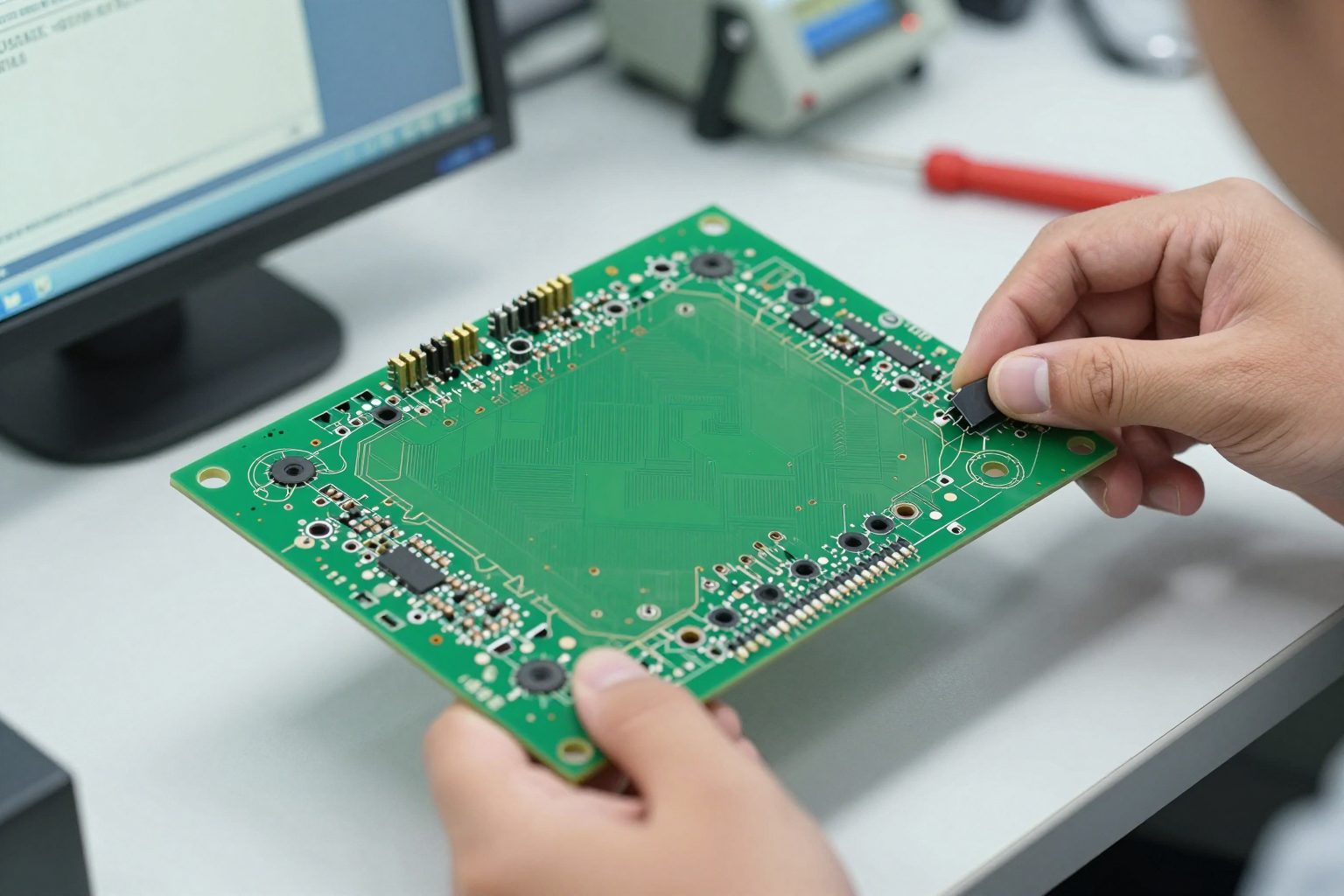
A board can be fabrication-ready and still not be assembly-ready. That is why PCB DFM should include PCBA-focused review before release, especially if the same package will be used for turnkey quoting or prototype assembly.
Assembly-readiness review should make connector access, test coverage, component spacing, and rework practicality visible before the board package is released for PCBA quotation or production.
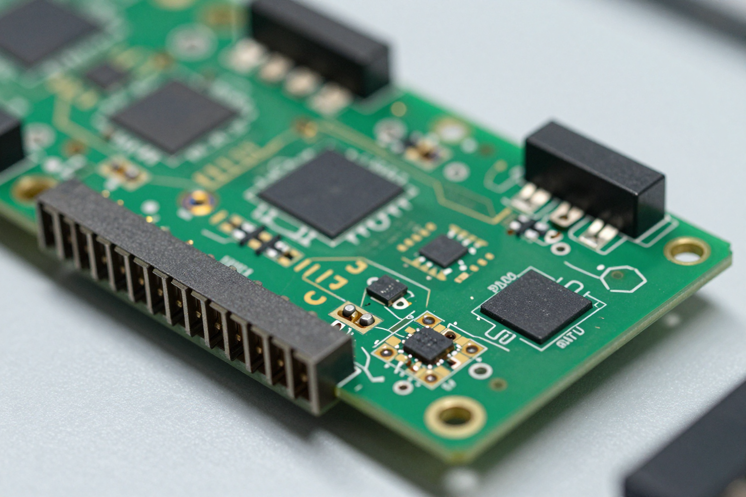
1. Check component spacing and placement accessibility
Review whether components are placed with enough margin for:
- pick-and-place access
- reflow consistency
- automated optical inspection (AOI) visibility
- probe access where testing matters
- manual rework on high-risk or high-value parts
Extremely dense placement may be necessary in some designs, but it should be intentional. If density is driven by layout convenience rather than product need, it often creates yield or service penalties later.
2. Review pad geometry against assembly method and package type
Pad shape and size affect solder behavior, not just land pattern compliance. Recheck:
- fine-pitch IC footprints
- BGA land patterns
- thermal pads and paste strategy assumptions
- connector anchor pads
- large component solder balance
Where the assembly process is sensitive, the safest path is to align design assumptions with the assembly house’s actual process window, not only with generic library defaults.
3. Confirm polarity, reference designators, and assembly intent are legible
Many avoidable assembly slowdowns come from documentation ambiguity rather than component shortage. Make sure the package communicates:
- polarity for all relevant parts
- orientation clarity for ICs, diodes, LEDs, and connectors
- readable reference designators where possible
- assembly notes for any special handling requirements
- DNI / DNP parts clearly identified
This is especially important for pilot runs, NPI builds, and mixed manual/automated assembly situations.
4. Think about testability before quoting, not after first build
Teams often delay test planning until prototypes arrive. That is late. During DFM review, decide whether the board needs:
- functional test access
- programming access
- debug headers or temporary pads
- test points for critical rails or signals
- fixture-friendly mechanical support
Even if production test will evolve later, basic test access should be considered before the design is released.
5. Review BOM realism and package availability in parallel
Strictly speaking, BOM sourcing is not a geometric DFM issue, but in real projects it is closely related. Some layout decisions become much harder to support if the intended packages are volatile, obsolete, or supplier-specific.
That is why the best pre-release review often combines PCB DFM and supply reality. If the design depends on parts that are hard to source, package alternatives and footprint implications should be considered before the board package is frozen.
Common DFM Mistakes That Delay Quotes or Cause Rework
Most DFM pain comes from patterns that repeat across otherwise different projects. Here are some of the most common ones.
Releasing files with implied rather than explicit intent
Examples include:
- no clear finished thickness callout
- impedance target mentioned in conversation but not in release data
- unclear drill tolerance expectations
- assembly notes that exist only in email threads
Manufacturers should not be asked to reverse-engineer design priorities from incomplete data.
Treating design rule check as full DFM
Passing CAD rules is necessary, but it is not equivalent to manufacturing review. CAD rules only verify what the rule deck knows to check. They do not confirm whether the full board package is practical, complete, and aligned with supplier process reality.
Sending inconsistent file packages
Quote delays often come from mismatches such as:
- drill file does not match fabrication drawing
- layer names conflict with stackup notes
- assembly drawings reference outdated revisions
- BOM and placement file are out of sync
These are avoidable release-management problems, not unavoidable factory issues.
Ignoring assembly impact during PCB release
If a board is likely to go to PCBA soon after fabrication, PCB-only DFM is incomplete. Teams that review only copper and drills often end up discovering assembly pain one step too late.
Waiting until quote feedback to ask basic manufacturability questions
A quote should refine risk, not reveal the first serious review. If the team already suspects stackup, drill, material, or component spacing may be marginal, it is better to raise those items before release.
How to Prepare a Cleaner Handoff Package for Your PCB Manufacturing Partner
A strong DFM review should end with a better release package, not just with comments inside the CAD tool. Before sending files out, make sure your handoff package is clean enough for a manufacturer to review without guesswork.
A practical release package should usually include:
- Gerber or equivalent fabrication data
- drill files
- stackup or fabrication notes
- board outline and mechanical details
- assembly drawing where applicable
- centroid / pick-and-place file
- BOM with clear manufacturer part numbers where available
- revision identifier and release date
- special process notes, if needed
Just as importantly, the package should be internally consistent. The board should not say one thing in the drawing, another in the stackup note, and a third in email context.
If you are preparing a board for supplier discussion, it also helps to provide concise review context such as:
- what is prototype-only versus production intent
- what dimensions are fixed versus negotiable
- which items are performance-critical
- whether assembly quote is expected together with fabrication review
- whether alternative materials or process suggestions are welcome
That kind of clarity improves not only quote speed, but also the quality of supplier feedback.
For teams that want a pre-release review before moving ahead, our capabilities page and contact page are the best starting points for a manufacturability discussion.
FAQ About PCB DFM Review
What is the difference between PCB DFM and PCBA DFM?
PCB DFM focuses on whether the bare board can be fabricated reliably, including stackup, traces, spacing, drills, mask, finish, and mechanical definition. PCBA DFM focuses on whether the populated board can be assembled, inspected, and tested reliably, including spacing, footprints, orientation clarity, access, and process sensitivity.
When should a PCB DFM checklist be used?
Ideally before files are released for quoting, prototyping, or production. If the review happens only after a supplier flags issues, the team is already reacting late.
Is DFM only important for complex HDI boards?
No. HDI boards often make DFM issues more visible, but even standard multilayer boards can lose time and yield because of incomplete stackup data, weak drill margin, mask problems, or unclear assembly release packages.
Should sourcing teams care about PCB DFM?
Yes. DFM quality affects quote clarity, supplier confidence, timeline predictability, and overall risk. Sourcing teams do not need to do every technical review themselves, but they benefit from knowing whether the release package is complete and factory-ready.
Can online tools replace a manufacturer DFM review?
No. Online tools are useful for early alignment and self-checking, especially for stackup and impedance assumptions, but they do not replace a real supplier review using production capability, materials, process constraints, and assembly context.
External References
For readers who want a neutral outside reference point, these two resources are useful starting points:
What is the biggest mistake teams make before manufacturing release?
Treating file export as the finish line. A board is not truly ready when design is complete in CAD. It is ready when the manufacturing package is clear, internally consistent, and strong enough to support fabrication and assembly without avoidable interpretation errors.
Conclusion
A good PCB DFM checklist is not bureaucracy. It is a practical tool for reducing iteration, improving quote quality, and catching issues while they are still cheap to fix.
Before sending a board to manufacturing, teams should review more than trace and drill rules. They should confirm stackup intent, drill margin, mask behavior, material assumptions, assembly constraints, test access, and release-package completeness. That is what turns a finished design into a manufacturable board.
For engineering and sourcing teams alike, the best outcome is simple: fewer surprises, cleaner supplier communication, and a faster path from design release to successful fabrication and assembly.