PCB Stackup Design Guide: How to Plan Layers, Reference Planes, and Manufacturing Constraints
SUNTOP Electronics
PCB stackup design is where electrical intent starts turning into a buildable board structure. Before routing gets too far, the team needs to decide how many layers the board really needs, which layers act as references, how power will be distributed, and what fabrication assumptions must stay stable from quote to production.
A weak stackup plan often creates avoidable confusion later. Layout may appear complete, but the manufacturer still has to ask basic questions about thickness, plane continuity, material family, impedance sensitivity, or whether the board can tolerate an alternate build approach. Good early stackup planning reduces that uncertainty before the files leave engineering.
The point of PCB stackup design is not to make a board look advanced. It is to build a layer structure that supports routing density, return-current control, EMI behavior, mechanical limits, and supplier review. That is why this planning should happen early, while the team still has room to adjust placement, layer roles, and manufacturing priorities instead of patching problems at release time.
This guide explains what PCB stackup design controls, how to assign layer roles, what material and impedance choices deserve early attention, and what information helps a manufacturer review the board faster.
What PCB Stackup Design Actually Controls in a Board Project
PCB stackup design controls more than the raw layer count. It defines the relationship between signal layers, copper planes, dielectric spacing, finished thickness targets, and routing behavior across the board. In practice, that means the layer plan affects both signal quality and manufacturability long before fabrication begins.
When a board moves beyond a simple two-layer layout, the stackup starts shaping several critical tradeoffs:
- whether important signals have a stable reference plane nearby
- whether power distribution can stay clean without fragmenting routing
- whether dense breakout areas have enough escape options
- whether the mechanical thickness target still supports the chosen layer structure
- whether the supplier can quote the board without guessing what is mandatory
This is why PCB stackup design should be treated as a working engineering decision, not a note added after routing. A board that depends on impedance control, dense BGAs, mixed-signal partitioning, or EMI-sensitive behavior usually needs a clearer stackup conversation than "four layers should be enough."
How to Assign Signal Layers, Planes, and Power Paths in PCB Stackup Design
Strong PCB stackup design starts by giving each layer a job. Some layers mainly carry signals, some exist to provide low-impedance reference return paths, and some help distribute power without forcing routing compromises everywhere else. If those roles stay vague, the stackup becomes harder to review and easier to break accidentally during layout changes.
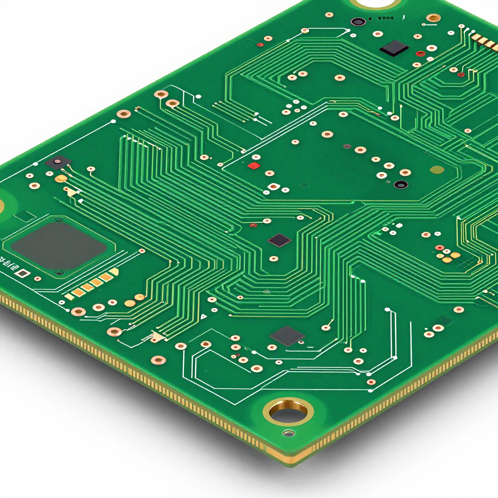
This close-up helps illustrate how clear layer roles and return-path planning should be reviewed before the stackup is released to fabrication.
A practical first pass is to identify:
- which signals are most sensitive to return-path quality
- which layers should remain as continuous ground references
- where power delivery needs broad copper support instead of narrow routed feeds
- which routing layers are likely to carry dense escape traffic or connector fanout
For early planning, the PCB Stackup Planner is a useful way to compare layer-role assumptions before the board reaches final release. When impedance is part of the discussion, the Online Impedance Calculator can help teams sanity-check dimensions and dielectric assumptions before supplier review.
PCB stackup design also needs awareness of how fields behave around routed traces. Outer-layer controlled lines are often discussed as microstrip structures, while internal controlled lines may behave more like stripline structures. The exact geometry still depends on the fabricator's materials and process window, but the design team should know which routing layers are intended to support that behavior.
The main goal is not academic perfection. It is to keep the board's critical routing close to stable references and avoid leaving plane continuity, copper balance, or return-current behavior to chance.
Material, Thickness, and Impedance Choices to Lock Early
The stackup plan becomes much more reliable when material and thickness expectations are discussed before quoting. Teams do not need to over-specify every detail too early, but they should know which assumptions are flexible and which ones directly affect performance or fit.
Start with the basics:
- target finished thickness, if the enclosure or connector system depends on it
- whether standard FR-4 is acceptable or whether a different dielectric family may be needed
- whether copper weight assumptions change thermal or current-carrying expectations
- whether impedance-controlled nets require tighter coordination with the fabricator
- whether the board is likely to need supplier-recommended adjustments to keep the stackup practical
If these points stay unresolved until release, PCB stackup design quickly turns into a negotiation instead of a plan. The fabricator may still help, but now the review cycle is slower because every change can affect routing, impedance, drilling, or board thickness together.
A useful discipline is to separate "electrically necessary" from "preferred if practical." That helps the supplier understand whether the stackup is locked for performance reasons or whether there is room for a more manufacturable alternative.
Common PCB Stackup Design Mistakes Before Quote or Release
Most PCB stackup design delays come from ambiguity, not from exotic technology. One common mistake is choosing a layer count without deciding what each layer must do. The board may be labeled as six layers, but there is no stable plan for reference planes, power regions, or dense routing areas.
Another frequent issue is treating PCB stackup design as independent from component placement. If large BGAs, connectors, noisy power sections, and sensitive analog areas are arranged without stackup consequences in mind, the routing later forces compromises that the stackup was never prepared to support.
Teams also lose time when the stackup intent is spread across too many places: a CAD preset, a fabrication note, a chat message, and a quote email that do not fully agree. That makes it hard for a manufacturer to know which assumption is current.
A few warning signs deserve attention before release:
- plane layers are heavily fragmented after routing pressure increases
- impedance-sensitive nets change reference behavior too often
- finished thickness targets conflict with the proposed dielectric structure
- material expectations are implied but not written clearly
- fabrication review would still need basic clarification before quoting starts
Good PCB stackup design is supposed to remove those questions early. If the supplier still has to reconstruct the board intent from scattered clues, the stackup package is not ready.
What to Send a Manufacturer for Stackup Review
This stackup work becomes more useful when it is documented clearly enough for someone outside the layout team to review it quickly. Before sending a board for quote or engineering feedback, make sure the release package explains not only the geometry of the stackup, but also the constraints that matter most.
A practical review package usually includes current fabrication files, drill data, the intended layer sequence, finished thickness expectations when known, any impedance-sensitive areas, and a short note about what parts of the stackup are fixed versus negotiable. If the project is still balancing manufacturability and performance tradeoffs, say so directly.
It also helps to explain the business context. Is this an early prototype where the team wants manufacturability feedback, or a near-release board where stackup changes would create major rework? That context changes how a supplier should review the design.
If your team wants feedback before locking the board, use the contact page to share the current stackup direction, known risk areas, and the questions you want answered. That usually leads to a better review than sending files with no explanation and waiting for uncertainty to come back as quote delay.
FAQ About PCB Stackup Design
When should PCB stackup design start?
PCB stackup design should start as soon as the board's complexity suggests that layer roles, reference planes, or impedance behavior will influence placement and routing choices. Waiting until the end usually makes changes more expensive.
Does PCB stackup design always require exotic materials?
No. Many projects use standard materials successfully. PCB stackup design only needs nonstandard material discussion when electrical, thermal, mechanical, or frequency requirements make ordinary assumptions too risky.
Can a manufacturer help refine PCB stackup design?
Yes. A manufacturer can often suggest more practical layer spacing, material options, or manufacturability adjustments. The better the initial PCB stackup design package is, the more useful that feedback becomes.
Conclusion
Good PCB stackup design gives the board a structure that electrical, layout, and manufacturing teams can all understand. When layer roles are clear, reference planes are protected, and stackup assumptions are documented early, the design moves toward quote and production with fewer avoidable surprises.
The goal is not to freeze every detail too soon. The goal is to make the important decisions visible early enough that the supplier can review the board as a real engineering package instead of a guess-filled file drop.