3D Printed Electronics Guide: Where It Fits, Limits, and How to Review It Against Standard PCB Manufacturing
SUNTOP Electronics
A 3D printed electronics program uses additive processes to place conductive, dielectric, or structural material directly onto a substrate or into a shaped part instead of following the full flow of standard etched PCB fabrication and later assembly. The idea sounds broad because it is broad. In practice, the term can describe several different approaches, from printed conductive traces on a formed surface to more experimental multilayer additive structures.
That range is exactly why teams should stay careful. The approach can be useful, but it is not a universal shortcut around normal PCB manufacturing rules. Material behavior, trace conductivity, mechanical durability, connector integration, and repeatability still decide whether the concept is practical.
For most product teams, the right question is not whether the technology is impressive. The better question is whether it solves a specific packaging, prototyping, or integration problem that a conventional rigid, flex, or assembled board handles poorly. If that answer is unclear, the safer path is often to compare the idea against a normal multilayer PCB design guide or a standard PCBA review before the architecture drifts too far.
This guide explains what 3D printed electronics usually means in real projects, where it fits best today, what technical limits should be reviewed early, and when a standard PCB or PCBA route is still the better manufacturing decision.
What 3D Printed Electronics Means and How It Differs from a Standard PCB Build
A conventional PCB program separates board fabrication and component assembly into mature, tightly controlled process steps. 3D printed electronics changes that model by creating conductive features through additive deposition, often on nontraditional shapes or with nontraditional material stacks.
That difference matters because the engineering questions change. Teams evaluating this route are often looking at shaped surfaces, integrated housings, low-volume prototypes, lightweight structures, or sensor concepts that do not fit neatly into a flat board plus enclosure model. The broader field overlaps with topics such as printed electronics and additive manufacturing, but product viability still depends on electrical performance and manufacturing control, not on novelty alone.
Compared with standard PCB fabrication, the additive route often brings more flexibility in form factor but less certainty in conductivity, layer precision, component attach strategy, and long-term production readiness. That tradeoff is acceptable in some programs, but it should be made deliberately.
Where 3D Printed Electronics Fits Best Today
The best 3D printed electronics use cases are usually narrow and practical rather than futuristic. Teams may explore the approach when they need electronics on a curved mechanical part, when early prototypes must combine structure and circuit paths, or when a sensor or antenna concept benefits from direct deposition on a non-flat surface.
Strongest fit is usually prototyping or specialized integration
In these cases, the method can reduce the number of separate mechanical and electrical parts in an early development loop. It can also help teams test packaging ideas before investing in a more mature production architecture.
Scale-up still needs a second decision
Even when the first prototype works, the additive route does not automatically become the best mass-production choice. Many teams still transition the concept into a conventional PCB, flex circuit, or hybrid assembly once the electrical and mechanical requirements are clearer. That handoff decision should happen early enough that the prototype path does not hide later sourcing or reliability risk.
Material, Conductivity, and Reliability Limits to Review Early
This is where 3D printed electronics becomes a real manufacturing decision instead of a concept demo. Conductive inks, printed metals, substrate compatibility, curing conditions, and environmental durability all influence whether the design can survive real use.
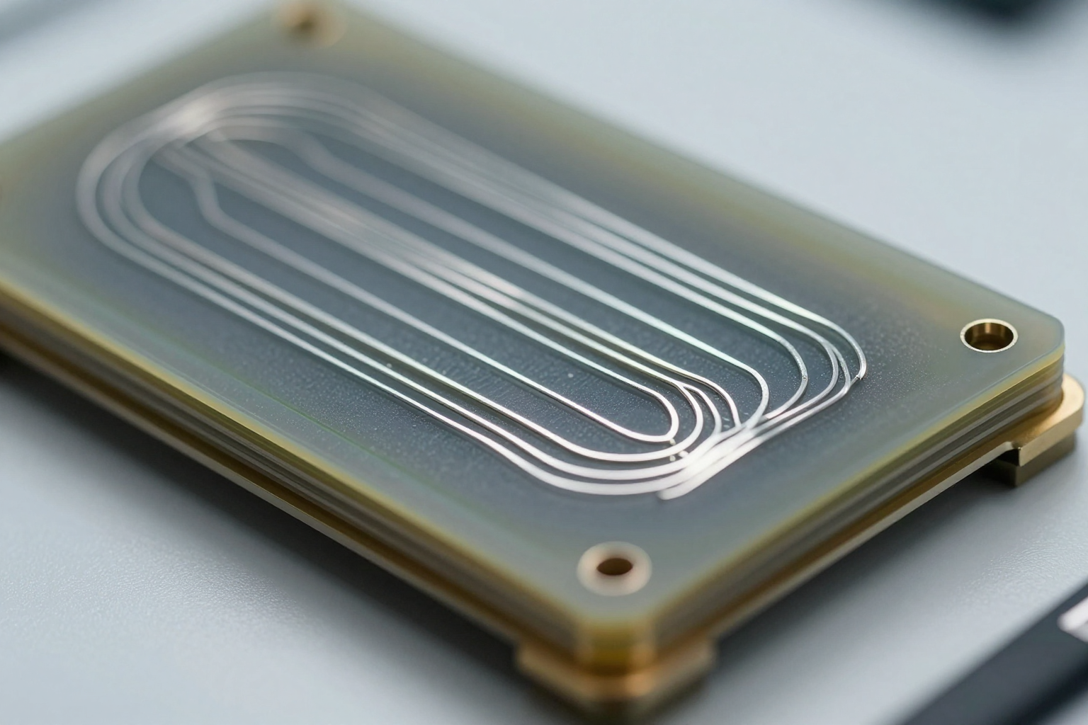
This close-up sample highlights how printed trace geometry and substrate build can differ from a standard copper PCB, which is why conductivity and durability still need early review.
The first limit is conductivity. A printed trace may be good enough for sensing, low-current routing, or proof-of-concept work while still behaving very differently from copper in a standard PCB stack. Resistance, heating, and signal loss should be reviewed against the real circuit demand rather than assumed to be acceptable.
The second limit is durability. Printed structures may react differently to flexing, abrasion, heat exposure, humidity, or repeated handling. If the design depends on connectors, shields, or later assembly steps, the team should also confirm how the printed features tolerate those downstream processes. This is one reason development teams often compare the concept with embedded-component ideas or more conventional integration paths before committing.
A third limit is qualification discipline. The approach may feel fast in the lab, but product teams still need test plans, material traceability, and a realistic view of repeatability. Industry conversations around additive manufacturing are useful background, but qualification should stay tied to the actual product environment, not to generic additive-manufacturing optimism.
Manufacturing and Supply-Chain Questions Before Choosing 3D Printed Electronics
A supplier conversation should start with intent, not with hype. If your team is exploring 3D printed electronics, define what problem it solves, what electrical load the printed features carry, what mechanical surface it lives on, and what production volume the program expects.
That information matters because the approach can create different sourcing questions from a standard PCB. Material availability, process consistency, inspection method, repairability, and fixture strategy may all change. If the product later transitions into a conventional board plus assembly flow, the team should understand that migration path up front instead of treating it as somebody else's future problem.
This is also the stage to ask whether the design really needs additive deposition or whether a conventional board, flex circuit, or mixed assembly route would be easier to quote and support. A short manufacturing discussion through the capabilities page or the contact page can prevent a lot of avoidable architecture churn.
When a Conventional PCB or PCBA Path Is Still the Better Choice
In many commercial products, standard PCB fabrication and assembly remain the better answer because they offer stronger process maturity, better supply-chain familiarity, and clearer qualification paths. If the design is fundamentally planar, current levels are meaningful, component density is conventional, and the product will need stable repeat production, 3D printed electronics may be more interesting than useful.
That does not make the additive route a failure. It simply means the technology is best treated as a targeted engineering option, not as a default upgrade over mature PCB manufacturing. The right comparison is always application-specific: geometry, electrical demand, inspection needs, production scale, and service risk.
FAQ About 3D Printed Electronics
Is 3D printed electronics replacing standard PCBs?
No. 3D printed electronics can support selected prototype or specialized integration cases, but standard PCB and PCBA workflows remain the stronger choice for many mainstream products.
Is 3D printed electronics only for research labs?
Not only, but the approach is still most convincing when the application has a real form-factor or integration reason for using it. Without that reason, a conventional manufacturing path is usually easier to scale and support.
When should a manufacturing partner be involved?
Early. The concept should be reviewed before the product architecture hardens, especially if the design may later shift into a conventional PCB or assembly route.
3D printed electronics can be valuable when it solves a real integration problem and the team treats materials, qualification, and production readiness seriously. The strongest programs compare the additive concept against standard PCB or PCBA options early, then choose the path that fits the actual product risk instead of the most eye-catching process story.