What is PCB Assembly? A Complete Guide to the PCB Assembly
Heros Rising
In today’s hyper-connected world, nearly every electronic device relies on a printed circuit board (PCB) to function. From smartphones and laptops to medical devices and automotive systems, PCBs serve as the backbone of modern electronics. But before these boards can power our gadgets, they must undergo a critical transformation known as PCB Assembly.
But what exactly is PCB Assembly, and why does it matter so much in the production of reliable, high-performance electronics?
This comprehensive guide will walk you through the entire PCB Assembly process, explain the most common assembly methods—including FPC Assembly, Rigid-Flex PCB Assembly, and HDI Assembly—and highlight best practices for ensuring quality and efficiency. Whether you're an engineer, product designer, or simply curious about how electronics are made, this article will give you a deep understanding of one of the most vital stages in electronic manufacturing.
Understanding PCB Assembly: The Foundation of Modern Electronics
At its core, PCB Assembly refers to the process of mounting and soldering electronic components onto a bare printed circuit board to create a fully functional unit, often referred to as a PCBA (Printed Circuit Board Assembly). Unlike a raw PCB, which is just a substrate with copper traces and pads, a completed PCBA contains resistors, capacitors, integrated circuits (ICs), connectors, and other active and passive parts that enable the board to perform specific functions.
The importance of precise and reliable PCB Assembly cannot be overstated. Even the most perfectly designed PCB layout will fail if components are improperly placed, misaligned, or poorly soldered. As consumer demand pushes toward smaller, faster, and more powerful devices, the complexity of PCB Assembly has increased dramatically—requiring advanced techniques, automated machinery, and rigorous quality assurance protocols.
Today’s electronics manufacturers use a variety of PCB Assembly methods tailored to different applications, performance requirements, and environmental conditions. These include surface mount technology (SMT), through-hole technology (THT), and hybrid approaches combining both. Additionally, specialized forms such as FPC Assembly (Flexible PCB Assembly), Rigid-Flex PCB Assembly, and HDI Assembly (High-Density Interconnect Assembly) have become essential for compact, high-speed, and space-constrained designs.
Let’s dive deeper into each stage of the PCB Assembly process and explore the technologies shaping the future of electronic manufacturing.
The Step-by-Step PCB Assembly Process
While the specifics may vary depending on the type of PCB and components involved, the general PCB Assembly process follows a well-defined sequence of steps. Each phase plays a crucial role in ensuring the final product meets electrical, mechanical, and reliability standards.
1. Solder Paste Application
The first step in most modern PCB Assembly lines is applying solder paste to the board's surface. Solder paste is a sticky mixture of tiny solder particles and flux, which helps clean metal surfaces during reflow and ensures strong solder joints.
A stencil—typically made of stainless steel—is aligned precisely over the PCB. This stencil has cutouts corresponding to the locations where surface-mount components will be placed. Using a squeegee, solder paste is spread across the stencil, filling the apertures and depositing small amounts of paste onto the component pads on the PCB.
Accuracy here is paramount; too little paste can lead to weak connections, while excess paste may cause bridging between adjacent pins, especially on fine-pitch components. Automated vision systems often inspect the applied paste to verify volume, alignment, and consistency before moving to the next step.
2. Component Placement (Pick-and-Place)
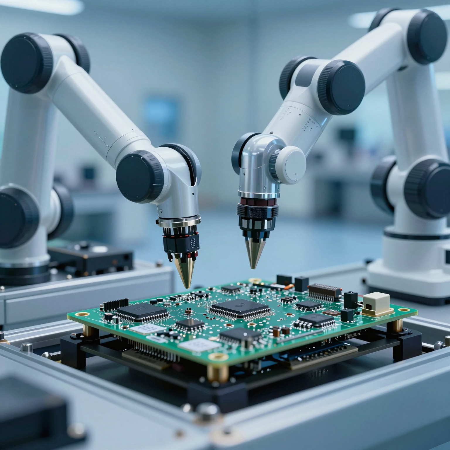
Once the solder paste is applied, the PCB moves to the pick-and-place machine—a high-speed robotic system responsible for placing surface-mount devices (SMDs) onto their designated pads.
These machines use vacuum nozzles to pick up components from reels, trays, or tubes and place them with micron-level precision. Advanced optical recognition systems ensure correct orientation and alignment by reading fiducial marks on the PCB and matching them against the component footprint data from the design files (usually Gerber or CAD).
Modern pick-and-place equipment can place tens of thousands of components per hour, making this stage highly efficient for mass production. However, even minor errors—such as reversed polarity on polarized capacitors or misaligned ICs—can render the board non-functional, emphasizing the need for careful programming and real-time inspection.
3. Reflow Soldering
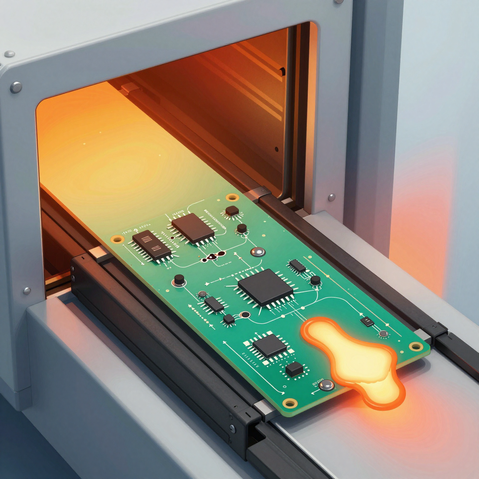
After all surface-mount components are placed, the PCB enters the reflow oven. Here, the board is gradually heated through several temperature zones:
- Preheat Zone: Slowly raises the board’s temperature to prevent thermal shock.
- Soak Zone: Evaporates solvents in the flux and activates it to clean oxidation from metal surfaces.
- Reflow Zone: Heats the board above the melting point of the solder (typically around 217°C for lead-free alloys), causing the solder paste to melt and form solid electrical and mechanical bonds.
- Cooling Zone: Cools the board at a controlled rate to solidify the solder joints without creating cracks or defects.
Thermal profiling is critical during reflow. An improper profile can result in tombstoning (where one end of a component lifts off the pad), cold solder joints, or damage to heat-sensitive components. Many manufacturers use thermocouples attached to test boards to monitor actual temperatures throughout the cycle.
4. Through-Hole Component Insertion
Not all components are surface-mounted. Some, particularly larger connectors, transformers, or components requiring higher mechanical strength, are inserted through holes drilled in the PCB. This method is known as through-hole technology (THT).
There are two main ways to assemble through-hole components:
- Manual Insertion: Used for low-volume or prototype builds, where technicians insert components by hand.
- Automatic Insertion Machines: For high-volume production, axial and radial insertion machines feed components into the board automatically.
After insertion, the leads extend through the bottom side of the board and must be soldered.
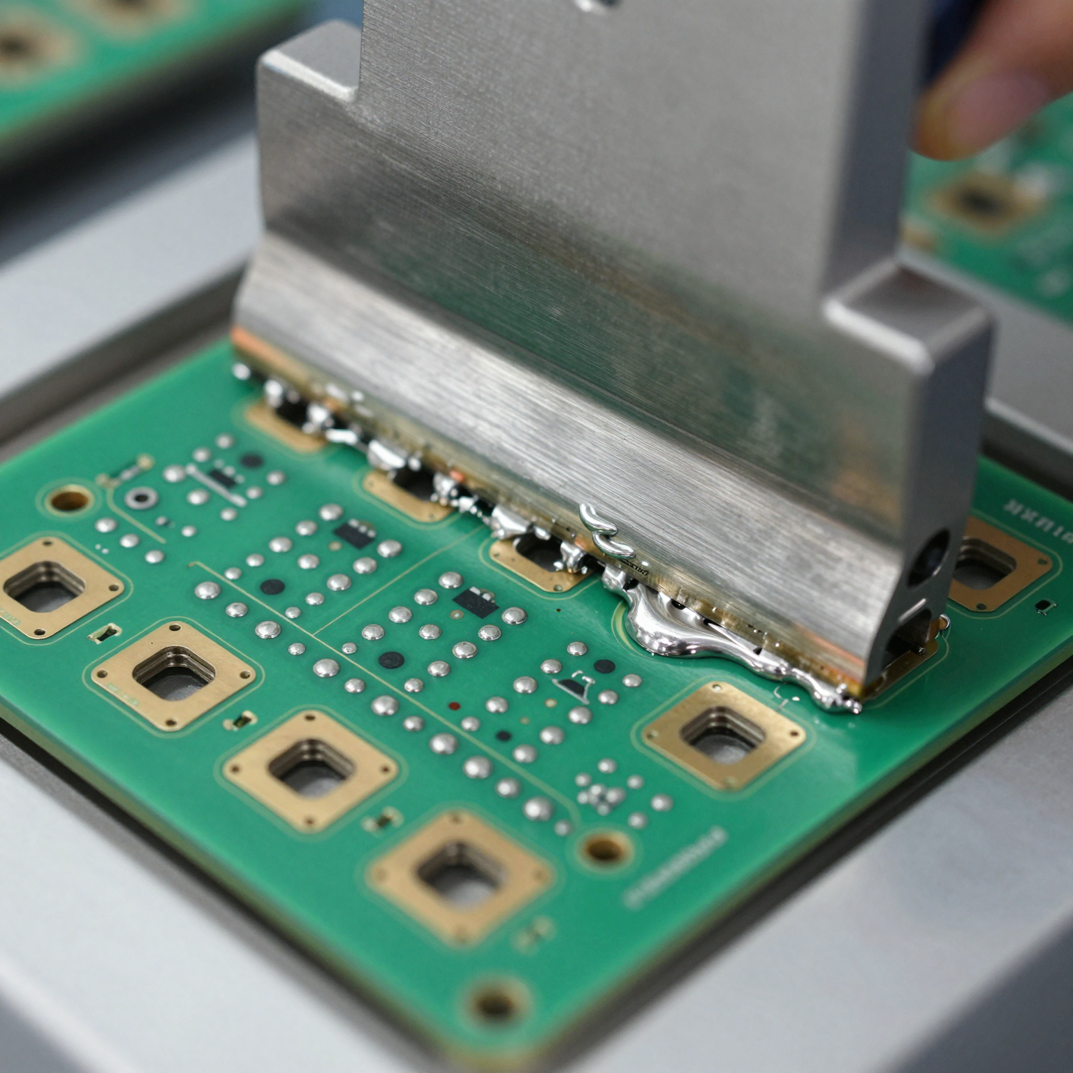
5. Wave Soldering or Selective Soldering
To solder through-hole components, most production lines use either wave soldering or selective soldering.
-
Wave Soldering: The PCB passes over a standing wave of molten solder. As the bottom of the board contacts the wave, solder flows up through the holes via capillary action, forming reliable joints. This method is fast and effective but not suitable for boards with sensitive surface-mount components already on the bottom side, as they could be damaged by the heat.
-
Selective Soldering: A more precise alternative, selective soldering uses a robot-controlled nozzle to apply solder only to specific through-hole joints. This allows mixed-technology boards (with SMT on both sides and THT components) to be assembled safely without exposing delicate parts to excessive heat.
Some advanced systems combine both processes in a single line, optimizing throughput and flexibility.
6. Inspection and Testing
Once all components are soldered, the board undergoes a series of inspections and tests to verify functionality and quality.
Common inspection methods include:
- Automated Optical Inspection (AOI): Uses high-resolution cameras and image processing software to detect missing components, misalignments, solder bridges, insufficient solder, and polarity errors.
- X-Ray Inspection (AXI): Especially important for inspecting hidden solder joints under components like Ball Grid Arrays (BGAs), where visual inspection is impossible.
- In-Circuit Testing (ICT): Probes individual components to check for opens, shorts, resistance values, capacitance, and other electrical parameters.
- Functional Testing (FCT): Simulates real-world operating conditions to ensure the assembled board performs as intended.
Defective units are flagged for rework, where technicians desolder faulty components and replace them manually or with semi-automated tools.
7. Cleaning and Final Coating (Optional)
Depending on the application, the finished PCBA may go through cleaning to remove flux residues, especially if water-soluble flux was used. In some cases, conformal coating—a thin protective polymer layer—is applied to shield the board from moisture, dust, chemicals, and thermal stress. This is particularly common in automotive, aerospace, and industrial environments.
With these seven steps complete, the PCB Assembly process yields a fully functional electronic module ready for integration into the final product.
Now that we’ve covered the standard workflow, let’s examine some of the specialized PCB Assembly techniques used in advanced electronics.
Exploring Key PCB Assembly Methods
As technology evolves, so do the demands placed on PCB Assembly. Miniaturization, higher speeds, flexible form factors, and tighter spacing require innovative solutions beyond traditional rigid boards with through-hole components. Let’s explore three advanced assembly types: FPC Assembly, Rigid-Flex PCB Assembly, and HDI Assembly.
FPC Assembly: Enabling Flexible and Compact Designs
FPC Assembly, or Flexible Printed Circuit Assembly, involves assembling components onto flexible substrates made from polyimide or similar materials. Unlike rigid PCBs, FPCs can bend, twist, and fold, making them ideal for applications where space is limited or dynamic movement is required.
Applications of FPC Assembly
- Wearable devices (smartwatches, fitness trackers)
- Foldable smartphones and tablets
- Medical implants and diagnostic equipment
- Automotive sensors and infotainment systems
- Consumer electronics (cameras, headphones)
Challenges in FPC Assembly
Working with flexible circuits introduces unique challenges:
- Handling Sensitivity: Thin FPCs are fragile and prone to tearing or creasing during handling.
- Registration Accuracy: Maintaining alignment during solder paste printing and component placement requires special tooling or carrier fixtures.
- Thermal Expansion Mismatch: Polyimide expands differently than solder, increasing the risk of joint failure under thermal cycling.
- Limited Heat Resistance: Excessive heat during reflow can warp or degrade the base material.
To overcome these issues, manufacturers often use stiffeners (reinforcement patches made of FR4 or metal) at component mounting areas and employ low-stress handling systems. Specialized reflow profiles with slower ramp rates help minimize thermal stress.
Despite the challenges, FPC Assembly offers unparalleled design freedom and is increasingly adopted in cutting-edge products.
Interested in learning more about designing for flexibility? Check out our guide on flexible PCB design best practices.
Rigid-Flex PCB Assembly: Combining Strength and Flexibility
Rigid-Flex PCB Assembly merges the durability of rigid boards with the adaptability of flexible circuits. These hybrid structures consist of multiple layers of rigid and flexible substrates laminated together into a single unit.
This approach eliminates the need for connectors and cables between separate boards, reducing weight, improving signal integrity, and enhancing reliability—especially in harsh environments.
Benefits of Rigid-Flex PCB Assembly
- Space Efficiency: Ideal for compact enclosures like drones, military gear, and portable medical devices.
- Improved Reliability: Fewer interconnects mean fewer potential points of failure.
- Enhanced Signal Performance: Shorter trace lengths reduce noise and crosstalk.
- Durability: Withstands vibration and repeated flexing better than discrete rigid boards connected by wires.
Assembly Considerations
Assembling rigid-flex boards presents additional complexities:
- Layer Registration: Ensuring perfect alignment between rigid and flexible sections during lamination and drilling.
- Component Placement Across Transitions: Components should not be placed directly over bend regions unless specifically designed for it.
- Special Fixturing: Custom jigs may be needed to support flexible portions during SMT and reflow.
- Testing Complexity: Requires sophisticated test fixtures due to 3D geometry.
Due to higher material and fabrication costs, Rigid-Flex PCB Assembly is typically reserved for high-reliability or mission-critical applications where performance outweighs cost considerations.
HDI Assembly: Powering High-Speed, Miniature Devices
HDI Assembly, or High-Density Interconnect Assembly, represents the pinnacle of miniaturized PCB technology. HDI boards feature finer lines and spaces, smaller vias (including microvias), higher connection pad density, and thinner materials compared to conventional PCBs.
These characteristics make HDI Assembly essential for smartphones, tablets, AI accelerators, and other high-performance computing devices.
Features of HDI Boards
- Microvias (typically <150 µm diameter)
- Blind and buried vias (connecting inner layers without going through the entire board)
- Sequential lamination (building up layers in stages)
- Higher I/O density BGA packages (e.g., 0.4 mm pitch)
Advantages of HDI Assembly
- Smaller Form Factor: Enables more functionality in less space.
- Better Electrical Performance: Reduced parasitic inductance and capacitance improve signal integrity.
- Increased Reliability: Shorter signal paths lower susceptibility to electromagnetic interference (EMI).
- Lower Power Consumption: Efficient routing reduces energy loss.
Challenges in HDI Assembly
- Precision Requirements: Micro-scale features demand ultra-fine solder paste stencils (often electroformed nickel) and high-vision placement systems.
- Microvia Reliability: Voids or cracks in microvias can lead to early failures under thermal cycling.
- Thermal Management: Denser components generate more heat in confined spaces.
- Test Access: Limited physical access complicates probing and debugging.
Manufacturers addressing HDI Assembly must invest in state-of-the-art equipment and adhere to strict process controls. For example, laser drilling is used to create microvias, and sequential build-up (SBU) processes allow complex multilayer stacking.
For deeper insights into this technology, read our article on HDI PCB technology.
Comparing SMT vs Through-Hole Assembly Techniques
Two primary methodologies dominate PCB Assembly: Surface Mount Technology (SMT) and Through-Hole Technology (THT). While many modern boards use a combination of both, understanding their differences is key to selecting the right approach for your project.
Surface Mount Technology (SMT)
SMT involves placing components directly onto the surface of the PCB, with their leads soldered to pads rather than inserted into holes. It became dominant in the 1980s due to its compatibility with automation and miniaturization trends.
Pros of SMT:
- Supports smaller components (down to 01005 size: 0.4 mm × 0.2 mm)
- Allows double-sided assembly
- Enables higher component density
- Faster and more cost-effective for large volumes
- Better performance at high frequencies due to lower parasitic effects
Cons of SMT:
- Less mechanically robust for heavy or frequently stressed components
- More susceptible to thermal stress and fatigue
- Requires precise equipment and skilled operators
- Hidden solder joints (e.g., BGAs) require X-ray inspection
Through-Hole Technology (THT)
THT predates SMT and involves inserting component leads through pre-drilled holes in the PCB and soldering them on the opposite side.
Pros of THT:
- Stronger mechanical bonds, ideal for connectors, switches, and transformers
- Easier manual assembly and repair
- Better heat dissipation for power components
- Suitable for prototyping and low-volume runs
Cons of THT:
- Larger footprint and lower component density
- Slower and more labor-intensive
- Requires drilling, increasing fabrication time and cost
- Not compatible with ultra-fine pitch or miniaturized designs
When to Use Which?
| Scenario | Recommended Method |
|---|---|
| High-volume consumer electronics | SMT |
| Prototypes and small batches | THT or mixed |
| Harsh environments (vibration, shock) | THT or reinforced SMT |
| High-frequency RF circuits | SMT |
| Large power components | THT |
| Space-constrained designs | SMT or HDI |
Many modern assemblies use a mixed-technology approach, leveraging the strengths of both methods. For instance, a smartphone might use SMT for processors and memory chips while incorporating a few through-hole screws or anchors for structural support.
To learn more about choosing between these methods, see our detailed comparison on SMT vs through-hole assembly.
Quality Control in PCB Assembly: Ensuring Reliability
No discussion of PCB Assembly would be complete without emphasizing the importance of quality control. Even the most advanced processes can produce defective units if not properly monitored and validated.
Why Quality Matters
A single faulty solder joint can compromise an entire system. In safety-critical industries like aerospace, automotive, and healthcare, failure is not an option. That’s why leading PCB Assembly providers implement multi-stage quality assurance programs.
Common Defects in PCB Assembly
- Solder bridges (short circuits between adjacent pins)
- Open circuits (insufficient solder or poor wetting)
- Tombstoning (asymmetric heating pulls one end of a component upward)
- Misplaced or missing components
- Cold solder joints (grainy appearance, poor conductivity)
- Voiding in BGA solder balls
- Delamination or warping due to moisture absorption (popcorning)
Key Quality Assurance Practices
-
Design for Manufacturability (DFM) Review: Engineers analyze the PCB layout before production to identify potential issues like inadequate spacing, incorrect pad sizes, or thermal imbalances.
-
Incoming Material Inspection: All PCBs, components, and solder materials are checked upon arrival for compliance with specifications.
-
Process Monitoring: Real-time monitoring of solder paste volume, placement accuracy, reflow profiles, and solder wave characteristics ensures consistent output.
-
Automated Inspection Systems:
- AOI detects visible defects post-SMT.
- AXI inspects internal joints in BGAs and QFNs.
- ICT verifies electrical continuity and component values.
-
Statistical Process Control (SPC): Tracks process variables over time to detect trends and prevent deviations.
-
Environmental Stress Screening (ESS): Boards are subjected to temperature cycling, vibration, and humidity to uncover latent defects.
-
Traceability and Documentation: Full lot tracking enables root cause analysis in case of field failures.
One effective way to maintain consistency is following a structured framework like the 6-step quality control process, which integrates checks at every stage—from incoming materials to final shipment.
Choosing the Right PCB Assembly Partner
Selecting a capable PCB Assembly manufacturer is crucial to bringing your product to market successfully. Look for partners who offer:
- Experience with your target industry (medical, automotive, industrial, etc.)
- Advanced capabilities in FPC Assembly, Rigid-Flex PCB Assembly, and HDI Assembly
- Robust quality management systems (ISO 9001, IPC-A-610 certification)
- Transparent communication and engineering support
- Scalable production capacity (prototyping to full-scale manufacturing)
If you're searching for a trusted PCB assembly manufacturer, consider visiting https://pcbassemblymfg.com/en to explore their full range of services, including PCB fabrication, electronic component sourcing, and PCB quality testing.
You can also review their PCB manufacturing capabilities or contact them directly to get a PCB quote.
Conclusion: The Future of PCB Assembly
PCB Assembly is far more than just attaching parts to a board—it’s a sophisticated blend of engineering, precision automation, and quality science. As electronic devices continue to shrink in size while growing in complexity, the demand for advanced assembly techniques like FPC Assembly, Rigid-Flex PCB Assembly, and HDI Assembly will only increase.
From wearable health monitors to autonomous vehicles and AI-powered edge devices, the success of tomorrow’s innovations depends on reliable, high-performance PCB Assembly processes.
By understanding the fundamentals—whether it’s mastering SMT vs through-hole trade-offs, navigating the intricacies of flexible circuits, or ensuring rigorous quality control—you’ll be better equipped to design, specify, and manufacture electronic products that meet the highest standards.
Stay informed, partner wisely, and embrace the evolving landscape of electronic manufacturing.