
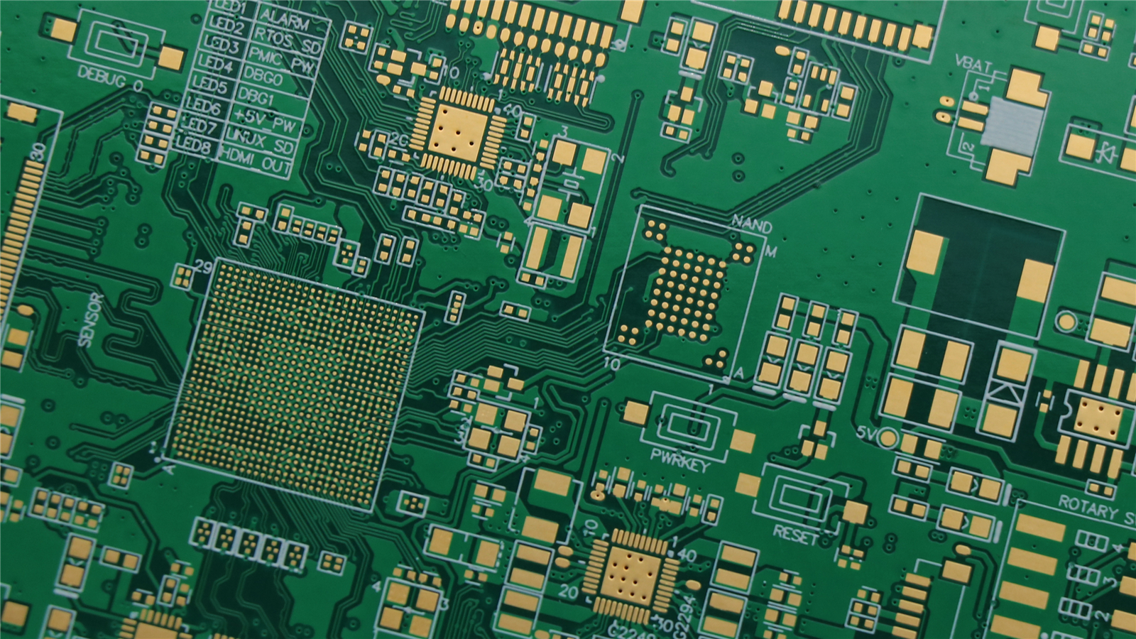
HDI
(76 条评论)
HDI
HDI PCB
具有微孔的高密度互连板,用于小型化高性能设备
主要特点
微孔
激光钻孔 ≤0.15mm
高密度
细间距元件
任意层HDI
先进互连
盘中孔
最大布线密度
技术规格
| 过孔尺寸 | 0.05mm - 0.15mm |
| 层数 | 最高20+层 |
| 最小线宽 | 0.075mm (3mil) |
| 堆叠 | 1+N+1 到 4+N+4 |
| 应用 | 智能手机, 平板电脑, 物联网 |
工程注意事项
报价前的制造审查
HDI boards need fabrication and assembly decisions to stay linked. A realistic stackup and via strategy should be reviewed before the layout is frozen.
- Confirm layer count, microvia structure, sequential lamination, via-in-pad requirements, and the escape strategy around fine-pitch packages.
- Review stackup, impedance-sensitive layers, copper balance, registration, solder mask, and inspection access before release.
- Align the fabrication build with BGA assembly, X-ray or AOI coverage, test access, and the product reliability stage.
典型应用
智能手机, 平板电脑, 物联网