
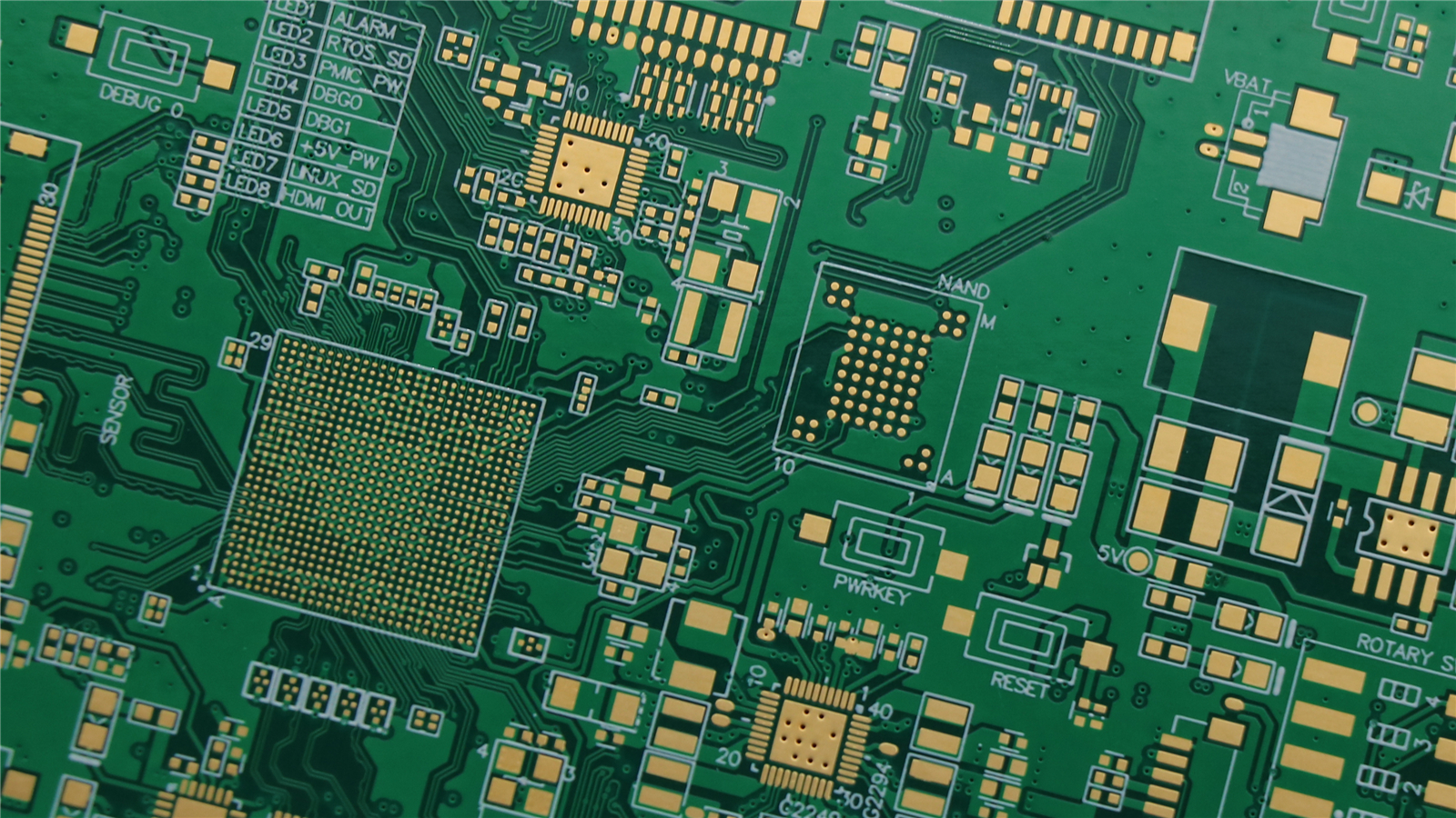
HDI PCB
(76 reviews)
HDI PCB
HDI PCB
첨단 전자 기기를 위한 고밀도 상호 연결 PCB
Key Features
마이크로 비아
레이저 드릴 비아 < 0.15mm
미세 라인
트레이스/공간 < 0.075mm
높은 신호 무결성
고속에 최적화됨
컴팩트 디자인
적은 공간에 더 많은 기능
Specifications
| 층 수 | 4-30층 |
| 비아 기술 | 블라인드, 베리드, 마이크로 |
| 종횡비 | 최대 10:1 |
| 최소 트레이스/공간 | 0.05mm/0.05mm |
| 자재 | High Tg FR4 |
Engineering considerations
Manufacturing review before quote
HDI boards need fabrication and assembly decisions to stay linked. A realistic stackup and via strategy should be reviewed before the layout is frozen.
- Confirm layer count, microvia structure, sequential lamination, via-in-pad requirements, and the escape strategy around fine-pitch packages.
- Review stackup, impedance-sensitive layers, copper balance, registration, solder mask, and inspection access before release.
- Align the fabrication build with BGA assembly, X-ray or AOI coverage, test access, and the product reliability stage.