
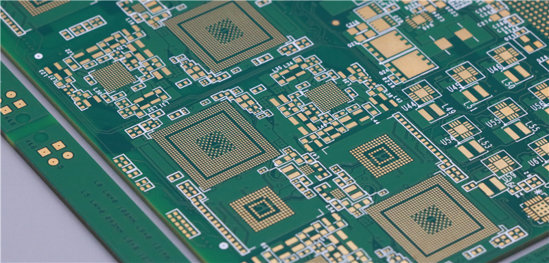
パワー基板
(145 reviews)
パワー基板
厚銅基板
パワーエレクトロニクスおよび自動車用途向けの、大電流対応基板
Key Features
大電流
最大200A
耐熱性
優れた放熱性
機械的強度
耐久性の向上
信頼性の高い接続
強力なビア
Specifications
| 銅箔厚 | 最大10oz (350µm) |
| 層数 | 2-20層 |
| 最小配線/間隔 | 0.2mm/0.2mm |
| 定格電流 | 最大200A |
| 用途 | 電源, 自動車, ソーラー |
エンジニアリング上の確認事項
見積り前の製造レビュー
Heavy copper designs should be reviewed against current capacity, thermal spreading, copper distribution, etching limits, drill capability, and the final assembly process before the stackup is fixed.
- Confirm finished copper weight, current target, allowable temperature rise, and whether the quoted value is starting foil or finished copper.
- Review via count, hole size, plating, copper balance, and thermal paths where high-current nets change layers.
- Share board thickness, isolation, terminal style, and assembly requirements because heavy copper changes drilling, etching, soldering, and panel planning.
代表的な用途
電源, 自動車, ソーラー