PCB Design for Assembly Guide: DFA Checks Before PCBA Release
SUNTOP Electronics
PCB design for assembly is the review step that asks whether a board can move from layout into real PCBA without avoidable friction. A design may pass electrical checks and still create assembly problems if placement is too dense, polarity is unclear, connectors block access, or the release package leaves the factory guessing.
That is why an assembly-focused review matters before quoting, prototype build, and volume release. Done well, it helps teams catch practical issues while changes are still cheap, instead of discovering them after stencils, procurement, or first articles are already in motion.
In day-to-day projects, this work usually overlaps with DFM, but it deserves its own focus. Bare-board manufacturability asks whether the board can be fabricated reliably. The assembly review asks whether the populated board can be placed, soldered, inspected, tested, and reworked with reasonable confidence.
This guide explains what this assembly-readiness review should cover, where teams often create avoidable PCBA risk, and how to prepare a cleaner handoff package before sending a board to a manufacturing partner.
What PCB Design for Assembly Means and Why It Matters Before PCBA Release
PCB design for assembly is the practical discipline of shaping a board so the assembly process works with the design instead of fighting it. In broader engineering language, it sits inside design for assembly, but PCB teams need board-specific checks tied to component placement, solder behavior, inspection access, and test planning.
A useful DFA review asks questions such as:
- Can placement equipment reach parts cleanly?
- Are polarity and orientation obvious enough for build and inspection?
- Do dense areas leave room for solder quality and later rework?
- Can the board be inspected and tested without awkward workarounds?
- Does the release package tell the assembly team what is intentional and what is flexible?
Those questions matter because many PCBA delays are not caused by advanced process failures. They come from simpler gaps: crowded connectors, weak fiducial strategy, incomplete BOM notes, ambiguous DNI parts, or footprints that are technically valid but poorly matched to the intended assembly method.
When it is handled early, engineering and sourcing teams can discuss those issues before quote feedback turns into a redesign loop. That creates a faster path into PCB assembly capabilities review and a cleaner conversation with the factory.
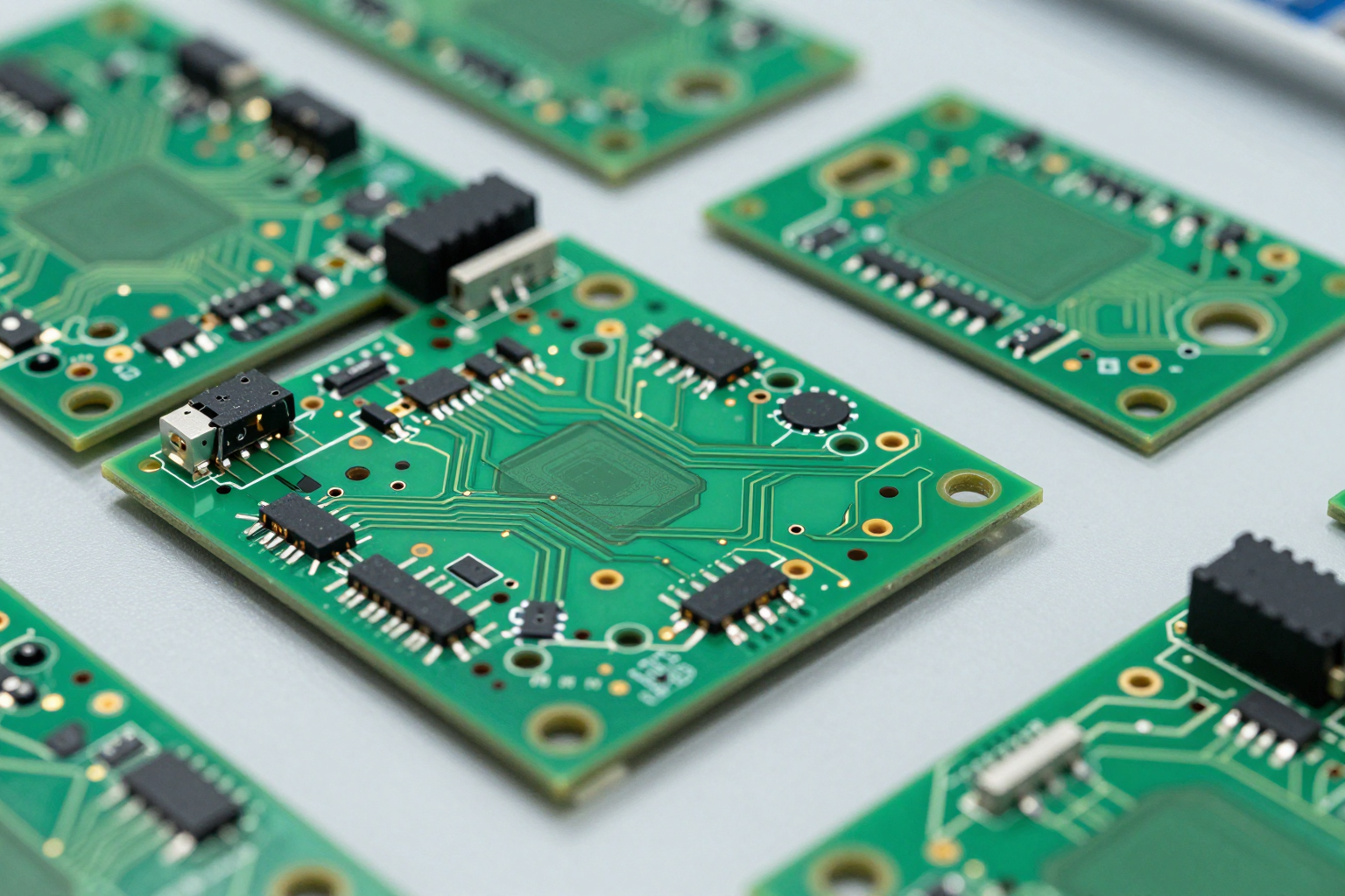
Component Placement Rules That Improve Assembly Yield and Inspection
Strong PCB design for assembly starts with placement, because placement controls much more than whether parts fit on the outline. It affects feeder access, soldering consistency, optical inspection, connector usability, test coverage, and serviceability later in the product life cycle.
The most useful placement review points are usually straightforward:
- keep enough spacing around fine-pitch and taller parts so adjacent components do not create soldering or inspection shadows
- avoid crowding connectors, switches, or large mechanical parts in ways that block nozzle access or later hand work
- place polarized parts so orientation is unambiguous in both the layout and the assembly drawing
- keep fiducials and tooling areas clear enough for stable alignment
- think about whether high-risk parts can still be reworked if the first build exposes an issue
This review also benefits from looking at groups of components instead of isolated footprints. A row of parts may be electrically logical yet hard to inspect if larger components hide smaller joints. A connector may fit mechanically yet still make probing, cleaning, or touch-up harder than expected.
Inspection visibility matters here as well. Processes such as automated optical inspection work best when solder joints and markings are not hidden by unnecessary placement conflicts. If a layout choice reduces inspection confidence, that should be treated as part of the DFA discussion, not as a downstream factory problem.
Footprints, Soldering, and Panel Details to Review Early
The review is not only about where parts sit. It is also about whether the land patterns, thermal behavior, and panel context give the soldering process a fair chance to succeed.
Start with footprint realism. Library parts may look acceptable in CAD while still needing review for package-specific assembly behavior. Fine-pitch ICs, BGAs, thermal pads, heavy connectors, and large passive parts all deserve a closer check before release. The goal is to confirm that footprint intent matches the actual assembly route instead of assuming that every default library choice is production-ready.
Soldering method matters too. If the board will go through reflow soldering, designers should think early about thermal balance, paste-sensitive pad structures, and whether component mix creates unusual process stress. If manual or selective operations are likely, the design should leave enough access and mechanical stability for those steps.
Panel-related choices can also change the real assembly experience. Review whether breakaway features, board edge clearances, and support for thinner or irregular outlines are practical for placement and depaneling. Even when panelization is finalized with the supplier, the original board design should not ignore how the assembly team will actually handle the product.
If a board includes heavy connectors, tall components near edges, or tight keepout regions, call those out before quote release. Assembly feedback is more useful when the team knows which layout features are fixed product requirements and which ones are open to improvement.
Documentation and BOM Details That Help the Assembly Team Move Faster
A technically sound layout can still produce a messy build if the documentation package is unclear. The assembly review should therefore include the handoff data, not just the PCB artwork.
At minimum, the assembly package should make these items easy to understand:
- BOM with clear manufacturer part numbers where available
- DNI or DNP status for optional parts
- centroid or pick-and-place data that matches the current revision
- assembly drawing with polarity and special notes where needed
- revision control that keeps fabrication, assembly, and BOM files aligned
- comments on sensitive parts, substitutions, or customer-supplied items when relevant
This is where the review often saves real time. A factory can quote and prepare more confidently when the release package is coherent. A sourcing team can also escalate fewer clarification loops when the design files and commercial package already tell the same story.
For teams reviewing the whole manufacturing handoff, it helps to pair this assembly-focused review with the existing PCB DFM checklist. The two reviews are related, but they solve different risks.
Common PCB Design for Assembly Mistakes That Cause Rework
Most assembly-readiness failures do not come from one dramatic error. They come from a stack of smaller decisions that look harmless in layout and become expensive during build preparation.
One common mistake is treating component spacing as a routing leftover. When placement is driven only by board density, the result may be difficult inspection, weak solder access, or awkward rework around connectors and shields.
Another mistake is assuming that a valid footprint is automatically a good assembly footprint. Teams should question whether pad geometry, thermal pads, and anchor structures reflect the intended process window, not just the library default.
Teams also lose time when documentation ambiguity is left for the factory to interpret. Missing polarity notes, outdated centroid data, or unclear optional-part handling can slow the first build even if the board itself is electrically correct.
A fourth mistake is ignoring test and programming access until after the prototype is built. Testability should be reviewed early enough to preserve practical access for debug, flashing, or functional checks.
Finally, some teams wait for quote feedback to perform the first real assembly review. By then, procurement and schedule pressure are already higher. The process is most valuable when it happens before the supplier has to discover basic readiness gaps on your behalf.
How to Prepare a Cleaner Handoff for Your PCBA Partner
A good PCB design for assembly review should end with a better release package and a clearer conversation with the assembly partner. The goal is not to document every thought in the layout process. The goal is to make the board easy to understand, quote, and build.
A cleaner handoff usually includes:
- current fabrication and assembly files for the same revision
- BOM, placement data, and assembly drawings that agree with each other
- clear notes on polarity, DNI parts, programming needs, and special handling
- brief context on what is prototype intent versus production intent
- early communication on parts or layout areas that may need assembly feedback
If the board has unusual spacing, large thermal masses, mixed technologies, or sourcing constraints, say so directly instead of leaving the factory to infer it. This review works best when engineering intent is legible.
When a team wants early review before freezing the package, the best next step is usually a short discussion through the contact page. That gives the PCBA partner a chance to flag practical build concerns while the design is still flexible.
FAQ About PCB Design for Assembly
Is PCB design for assembly the same as PCB DFM?
Not exactly. PCB design for assembly focuses on populated-board readiness, including placement, soldering, inspection, test access, and assembly data quality. PCB DFM is broader and also covers bare-board fabrication topics such as stackup, drills, copper spacing, and board definition.
When should PCB design for assembly happen?
Ideally before files are released for PCBA quoting or prototype build. The earlier this review happens, the easier it is to fix spacing, polarity, documentation, and access problems without schedule pain.
Do prototype boards still need PCB design for assembly review?
Yes. Prototype runs are exactly where this review can save time, because early builds often expose orientation mistakes, weak rework access, and documentation gaps that are still fixable before a larger release.
What should sourcing teams look for in PCB design for assembly?
They do not need to review every footprint in detail, but they should check whether the package is coherent, whether optional parts are clear, and whether the supplier has enough information to quote and prepare the build without repeated clarification.
Conclusion
PCB design for assembly is a practical readiness review, not extra paperwork. It helps teams check whether a board can be placed, soldered, inspected, tested, and supported without avoidable confusion.
When the review is done before release, quote cycles get cleaner, first builds get fewer surprises, and engineering discussions with the PCBA partner become more useful. That is the real value: fewer preventable loops between layout completion and a board that is actually ready to build.