BGA Assembly Challenges and Solutions
David Lee
As electronic devices continue to evolve—becoming faster, smaller, and more powerful—the demand for high-density interconnects has never been greater. Ball Grid Array (BGA) packages have emerged as a critical solution in modern PCB design, offering superior electrical performance, thermal management, and space efficiency over traditional packaging technologies. However, while BGA technology enables next-generation electronics, it also introduces unique manufacturing complexities.
At SUNTOP Electronics, a leading PCB assembly manufacturer, we specialize in overcoming these challenges through precision engineering, advanced equipment, and rigorous BGA Quality Control protocols. In this comprehensive guide, we’ll explore the most common BGA assembly challenges, their root causes, and proven BGA Solutions that ensure reliability, yield, and long-term product success.
Whether you're an engineer designing your first BGA-based board or a procurement manager sourcing high-reliability assemblies, understanding the intricacies of BGA integration is essential. Let’s dive into what makes BGA both revolutionary—and demanding.
What Is BGA? Understanding the Basics
Definition and Structure of BGA Packages
Ball Grid Array (BGA) is a type of surface-mount packaging used for integrated circuits. Unlike quad flat packs (QFPs) that use leads around the perimeter, BGAs utilize an array of solder balls on the underside of the package to connect to the printed circuit board (PCB). These solder balls are arranged in a grid pattern, allowing for hundreds—or even thousands—of connections within a compact footprint.
The structure typically includes:
- A substrate made of ceramic or organic material
- Solder balls (usually tin-lead or lead-free alloys like SAC305)
- An encapsulated die connected via wire bonds or flip-chip technology
This design provides several advantages:
- Higher pin count in limited space
- Shorter electrical paths — reduced inductance and improved signal integrity
- Better thermal dissipation due to direct contact with the PCB
- Improved mechanical stability under thermal cycling
Why BGA Is Used in Modern Electronics
BGAs are now standard in applications requiring high performance and miniaturization:
- Consumer electronics: Smartphones, tablets, wearables
- Networking hardware: Routers, switches, base stations
- Automotive systems: ADAS, infotainment, engine control units
- Industrial automation: PLCs, robotics, vision systems
- Medical devices: Imaging equipment, patient monitors
Because BGAs support higher I/O density without increasing package size, they enable Moore’s Law-style advancements in computing power. But with great capability comes great complexity—and significant manufacturing hurdles.
Common BGA Assembly Challenges
Despite their benefits, BGA components pose notable difficulties during PCB assembly. The hidden nature of the solder joints—located beneath the chip—makes inspection and rework extremely challenging. Below are some of the most prevalent issues encountered during BGA assembly.
1. Solder Bridging

and Short Circuits
One of the most frequent defects in BGA assembly is solder bridging, where adjacent solder balls merge during reflow, creating unintended electrical connections. This can occur due to:
- Excessive solder paste deposition
- Poor stencil design (aperture size too large)
- Misalignment during placement
- Uneven heating profiles causing slumping
Since the joints are not visible post-reflow, detecting shorts requires specialized tools such as X-ray inspection.
Pro Tip: Use laser-cut stencils with trapezoidal walls to improve paste release consistency and reduce bridging risk.
2. Insufficient Solder
Joint (Opens)
On the opposite end of the spectrum, insufficient solder volume leads to open circuits. Causes include:
- Incomplete coalescence of solder balls and pads
- Oxidation on solder balls or PCB lands
- Poor wetting due to incorrect flux activity
- Pad cratering or delamination
These defects result in intermittent connections or complete failure, often only surfacing after thermal stress or mechanical shock.
3. Voiding in Solder Joints
Voids—pockets of trapped gas within the solidified solder joint—are common in BGA assemblies. While minor voiding (<25%) may be acceptable per IPC-A-610 standards, excessive voids compromise:
- Thermal conductivity
- Mechanical strength
- Long-term reliability
Primary contributors to voiding:
- Volatile outgassing from flux residues
- Rapid ramp rates in reflow profile
- Substrate moisture absorption (especially in plastic BGAs)
Moisture-sensitive components must be baked before assembly to prevent "popcorning" and internal void formation.
4. Coplanarity and Placement Accuracy Issues
Coplanarity refers to how uniformly the solder balls sit relative to the bottom surface of the BGA package. Non-coplanar balls can lead to poor contact with the PCB, resulting in opens or weak joints.
Factors affecting coplanarity:
- Warpage of the BGA package due to thermal mismatch
- Improper storage conditions (humidity exposure)
- Mechanical damage during handling
Additionally, accurate placement is crucial. Even micron-level misalignment can cause incomplete connections, especially with fine-pitch BGAs (e.g., 0.4mm pitch).
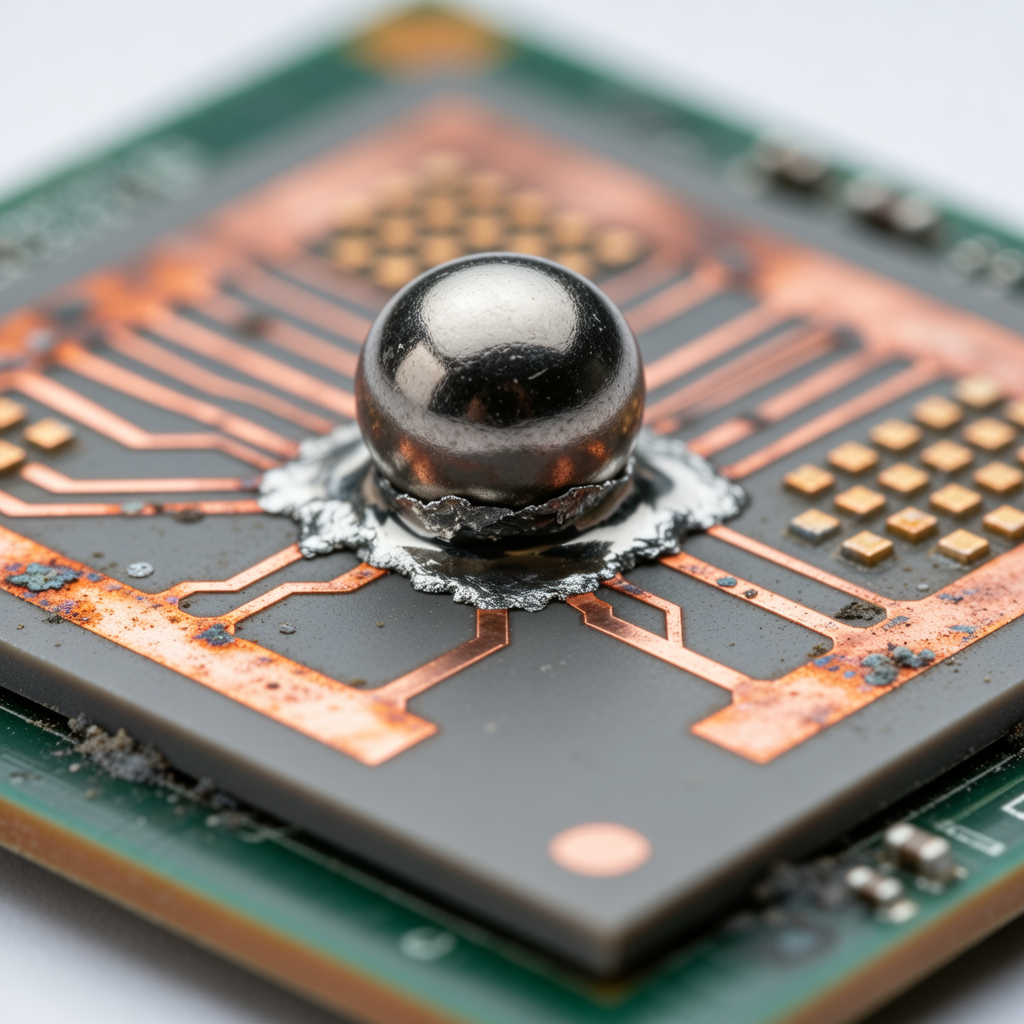
5. Head-in-Pillow

(HiP) Defects
A particularly insidious defect known as Head-in-Pillow (HiP) occurs when the solder ball ("head") fails to fully merge with the molten solder paste on the PCB pad ("pillow"). Visually, it resembles a partially flattened sphere resting on top of unmixed solder.
Root causes:
- Component warpage lifting the ball off the pad during reflow
- Mismatched thermal profiles between top and bottom sides of the board
- Out-of-specification solder paste rheology
- Delayed component settling due to surface tension imbalance
HiP defects are notoriously difficult to detect without cross-sectioning or 3D X-ray analysis.
6. Thermal Stress and Fatigue Cracking
During operation, repeated thermal cycling causes expansion and contraction at different rates between the silicon die, package substrate, and PCB. Over time, this leads to fatigue cracking in solder joints—particularly at the outermost rows of the array where strain is highest.
This issue is exacerbated by:
- Large CTE (Coefficient of Thermal Expansion) mismatch
- Thick PCBs or rigid substrates
- Lack of underfill or conformal coating
- High-power environments (e.g., automotive under-hood applications)
Without mitigation, fatigue cracks grow until the joint fails electrically or mechanically.
How SUNTOP Electronics Addresses BGA Assembly Challenges
As a full-service PCB assembly services provider, SUNTOP Electronics leverages cutting-edge technology, strict process controls, and deep technical expertise to deliver robust BGA solutions. Our approach spans design consultation, precision manufacturing, and comprehensive BGA Quality Control—ensuring every assembly meets the highest standards of reliability.
Let’s examine how we tackle each challenge head-on.
Advanced Stencil Design and Solder Paste Printing
Precision begins with consistent solder paste application. We employ:
- Laser-cut stainless steel stencils with nano-coatings to enhance paste release
- Aperture designs optimized using statistical modeling and empirical data
- Automated stencil cleaners to maintain print quality across production runs
Our SPI (Solder Paste Inspection) systems use 3D laser scanning to verify volume, height, and position accuracy—catching printing defects before component placement.
By maintaining tight tolerances (±10% of target volume), we minimize risks of bridging and insufficient joints.
High-Accuracy Pick-and-Place Machines
We utilize state-of-the-art Siemens ASM and Fuji NXT III pick-and-place machines capable of placing BGAs with sub-micron accuracy. Features include:
- Vision systems with multi-point alignment for true centroid correction
- Adaptive nozzle selection based on component weight and size
- Real-time feedback loops that adjust placement force and angle
For ultra-fine-pitch BGAs (down to 0.3mm), we implement closed-loop verification to ensure zero misregistration.
Optimized Reflow Profiles with Thermal Profiling Software
Thermal management is central to successful BGA assembly. We develop custom reflow profiles using KIC Navigator software, which models heat transfer dynamics across complex multilayer boards.
Key parameters we optimize:
- Ramp rate (to avoid thermal shock)
- Soak duration (for uniform flux activation)
- Peak temperature (to ensure complete melting without damaging components)
- Cooling slope (to promote fine grain structure)
Each profile is validated using thermocouples placed directly on BGA packages and monitored in real time.
Moreover, all moisture-sensitive devices (MSDs) are stored in dry cabinets and baked according to JEDEC standards prior to assembly.
X-Ray Inspection and 3D AXI for Hidden Joint Analysis
Given that BGA joints are invisible post-assembly, visual inspection is impossible. That’s why SUNTOP employs automated X-ray inspection (AXI) as a core part of our BGA Quality Control process.
Our Nordson DAGE XD7600 system offers:
- 2D and 3D computed tomography (CT) imaging
- Void percentage measurement per IPC-7095 guidelines
- Ball displacement and coplanarity analysis
- Detection of head-in-pillow, bridging, and opens
All inspections are documented and traceable, supporting AS9100, ISO 13485, and automotive-grade quality requirements.
Underfill Application for Enhanced Reliability
To combat thermal fatigue and mechanical stress, we offer underfill dispensing as an optional but highly recommended process for mission-critical applications.
Underfill is a polymer resin injected along the edges of the BGA after reflow. Capillary action draws it underneath the package, where it cures to form a rigid mechanical bond between the component and PCB.
Benefits:
- Reduces stress on individual solder joints by up to 90%
- Prevents crack propagation
- Improves resistance to vibration and drop impacts
- Extends operational life in harsh environments
Commonly used in aerospace, defense, medical, and industrial sectors.
Rework and Repair Capabilities
Even with best practices, occasional defects occur. SUNTOP maintains a dedicated BGA rework station equipped with:
- Precision infrared and convection heating
- Vacuum pickup tools with thermal sensors
- Microscopes and alignment cameras
- Pre-programmed rework profiles for various BGA types
Our technicians follow IPC-7711/7721 standards for safe removal, cleaning, reballing (if needed), and reinstallation—minimizing risk to surrounding components and the PCB itself.
Reballed components undergo full X-ray inspection before being returned to the line.
Ensuring BGA Quality Control: Our Multi-Layered Approach
Quality isn’t an afterthought—it’s built into every stage of our PCB assembly workflow. At SUNTOP, we apply a layered BGA Quality Control strategy that combines preventive measures, real-time monitoring, and final validation.
Layer 1: Design for Manufacturability (DFM) Review
Before any production begins, our engineering team conducts a thorough DFM review focused specifically on BGA compatibility. We analyze:
- Land pattern dimensions vs. manufacturer specifications
- Solder mask defined (SMD) vs. non-solder-mask-defined (NSMD) pads
- Via-in-pad plating and tenting methods
- Thermal relief design for ground planes
- Keep-out zones for nearby components
Using tools like Altium Designer and Valor Process Preparation, we identify potential issues early—saving time, cost, and yield downstream.
Clients receive detailed reports with actionable recommendations, ensuring manufacturability from day one.
Layer 2: Incoming Material Inspection
All raw materials—including BGA components—are inspected upon arrival. We check for:
- Date codes and moisture sensitivity levels (MSL)
- Physical damage or deformation
- Package warpage using optical profilometers
- Certificate of Conformance (CoC) and lot traceability
Components classified as MSL3 or higher are immediately moved to dry storage with humidity below 10% RH.
Layer 3: In-Line Process Monitoring
Throughout the assembly line, automated systems continuously monitor key variables:
- SPI results for paste volume deviation
- Placement offset data from vision systems
- Reflow profile compliance (with alerts for anomalies)
- Conveyor speed and environmental conditions
Any parameter outside predefined limits triggers an immediate stoppage and root cause investigation.
Layer 4: Final Testing and Validation
Post-assembly, every board undergoes functional testing tailored to its application. For BGA-heavy designs, we integrate additional verification steps:
- Flying probe or bed-of-nails testing for connectivity
- Boundary scan (JTAG) for inaccessible nodes
- Burn-in testing under elevated temperatures
- Environmental stress screening (ESS) including thermal cycling and vibration
Combined with AXI results, this creates a complete picture of product health.
You can learn more about our 6-step quality control process that ensures zero-defect delivery across all projects.
Best Practices for Successful BGA Implementation
While manufacturers play a critical role, designers and engineers can significantly influence BGA success through thoughtful design choices. Here are key best practices:
Optimize Land Patterns According to IPC Standards
Always follow IPC-7351B guidelines for land pattern creation. For NSMD pads (recommended for most BGAs), ensure:
- Copper pad diameter = 0.3–0.5 × pitch
- Solder mask opening slightly larger than copper to allow wicking
- Adequate spacing to prevent bridging
Avoid overly large pads, which increase the risk of tombstoning and uneven wetting.
Use Via-in-Pad Strategically
Vias placed inside BGA pads help route high-density traces—but they must be properly plated and filled to prevent solder wicking into the hole.
Recommended approach:
- Plated and filled vias with non-conductive epoxy
- Tented over with solder mask
- Avoid open vias unless backfilled
This prevents voiding and ensures consistent solder joint formation.
Implement Proper Thermal Management
High-power BGAs generate significant heat. Incorporate:
- Internal thermal planes connected to the BGA ground array
- Thermal vias beneath the center pad (if applicable)
- Heatsinks or thermal interface materials (TIMs)
Ensure adequate airflow in the final enclosure to dissipate heat effectively.
Plan for Testability and Debugging
With many signals inaccessible under the BGA, plan early for test access:
- Include JTAG headers or boundary-scan chains
- Add test points for critical power rails and clocks
- Consider boundary scan-compatible ICs when possible
Collaborate with your PCB assembly manufacturer during layout to ensure test coverage.
Case Study: High-Density FPGA BGA Assembly for Industrial Automation
Client: European industrial controller OEM
Challenge: Assemble a 1,152-ball FPGA (0.8mm pitch) onto a 12-layer HDI PCB with tight timing constraints
Requirements: Zero defects, full traceability, extended operating temperature (-40°C to +85°C)
Solution Implemented by SUNTOP:
- Conducted joint DFM session with client to validate stack-up, via design, and impedance control
- Fabricated laser-drilled microvias with filled and capped construction
- Applied precision-printed solder paste using 4-mil electroformed stencil
- Placed FPGA using Siemens SX7 with dual-camera alignment
- Executed custom reflow profile with nitrogen atmosphere to reduce oxidation
- Performed 3D AXI inspection with automatic void mapping and reporting
- Applied capillary underfill for enhanced mechanical reliability
- Ran 72-hour burn-in test followed by functional verification
Outcome:
- First-pass yield: 99.8%
- No field returns after 18 months of deployment
- Client expanded partnership to include full turnkey PCBA services
This project exemplifies how combining advanced capabilities with disciplined BGA Solutions leads to real-world success.
Choosing the Right PCB Assembly Partner for BGA Projects
Not all contract manufacturers are equally equipped to handle BGA assembly. When evaluating partners, ask:
- Do they have dedicated AXI systems?
- Are their reflow ovens profiled and calibrated regularly?
- Can they provide evidence of successful BGA projects?
- What underfill and rework options do they offer?
At SUNTOP Electronics, we pride ourselves on transparency, capability, and customer collaboration. With decades of experience in complex PCB assembly, we’ve developed a reputation for solving tough problems—especially those involving dense, high-speed, or mission-critical boards.
We serve industries ranging from telecommunications to medical devices, always adhering to the highest quality benchmarks. Learn more about the industries served by PCB manufacturer to see if we align with your sector.
Conclusion: Mastering BGA Assembly Through Expertise and Technology
BGA technology continues to drive innovation in electronics—but mastering its assembly demands more than just equipment. It requires deep process knowledge, meticulous attention to detail, and a commitment to continuous improvement.
From preventing solder bridging to eliminating head-in-pillow defects, BGA assembly challenges are numerous—but surmountable. By partnering with an experienced PCB assembly manufacturer like SUNTOP Electronics, you gain access to:
- Advanced manufacturing infrastructure
- Proven BGA Solutions
- Rigorous BGA Quality Control procedures
- End-to-end support from design to delivery
Whether you’re prototyping a new concept or scaling up production, we’re here to help you achieve flawless BGA integration.
Ready to discuss your next project? Contact PCB manufacturer today or get a PCB quote for your upcoming BGA-based design.
Together, let’s build smarter, smaller, and more reliable electronics.