Prototype PCB Assembly: A Complete Guide to PCB Sampling and Rapid Development
Winnie King
In the fast-evolving world of electronics, speed, accuracy, and reliability are non-negotiable. Whether you're a startup developing a groundbreaking IoT device or an established company iterating on existing technology, the journey from idea to market-ready product hinges on one critical phase: Prototype PCB Assembly.
This stage allows engineers and designers to validate their circuit designs, test functionality, and identify potential flaws before moving into full-scale manufacturing. It’s not just about building a board—it's about de-risking your project, saving time and money, and ensuring that your final product performs as intended.
What Is Prototype PCB Assembly?
Prototype PCB Assembly refers to the process of assembling electronic components onto a printed circuit board (PCB) for the purpose of testing and validation. Unlike mass production runs, prototype assemblies are typically produced in small quantities—ranging from a single unit to several hundred boards—allowing developers to evaluate electrical performance, mechanical fit, thermal behavior, and manufacturability.
The goal is simple: build a working model that mirrors the intended final product as closely as possible. This enables real-world testing under actual operating conditions, which simulations alone cannot fully replicate.
Why Prototyping Matters
Skipping the prototyping phase may seem like a shortcut, but it often leads to costly mistakes down the line. Consider this:
- Design errors caught during PCB Sample testing can prevent expensive redesigns later.
- Component placement issues revealed early improve yield rates in volume production.
- Firmware and hardware can be co-developed and debugged simultaneously.
- Regulatory compliance and safety standards can be preliminarily assessed.
In short, Prototype PCB Assembly acts as a bridge between theoretical design and scalable manufacturing.
The Role of PCB Sampling in Product Development
A key component of successful prototyping is PCB Sampling—the creation of a limited batch of circuit boards designed to represent the final product. These samples serve multiple purposes across different stages of development.
1. Proof of Concept (PoC)

At the earliest stage, a basic PCB Sample helps demonstrate that the core idea works. This might involve minimal functionality but proves the feasibility of the underlying electronics.
2. Functional Testing
Once the initial concept is validated, more refined prototypes undergo rigorous functional testing. Engineers assess signal integrity, power consumption, heat dissipation, and response times. Any anomalies detected here can lead to immediate design adjustments.
3. Design for Manufacturability (DFM)
Even the most elegant circuit design can fail if it’s not manufacturable at scale. During PCB Sampling, manufacturers analyze the layout for potential production issues such as:
- Insufficient trace spacing
- Incorrect pad sizes
- Component accessibility for automated assembly
- Thermal relief considerations
Feedback from this stage ensures that when the product moves to high-volume production, yields remain high and defects low.
4. Client and Stakeholder Review
Physical prototypes provide tangible evidence of progress. They’re essential for investor presentations, client approvals, and internal reviews. A working PCB Sample communicates far more effectively than schematics or renderings ever could.
Key Steps in the Prototype PCB Assembly Process
Understanding the workflow behind Prototype PCB Assembly helps set realistic expectations and improves collaboration with your manufacturing partner.
Step 1: Design Finalization and File Submission
Before any physical work begins, the design must be finalized. This includes:
- Schematic capture
- PCB layout (using tools like Altium Designer, KiCad, or Eagle)
- Generation of Gerber files, drill files, and bill of materials (BOM)
These files are submitted to the manufacturer for review. Many providers offer free DFM checks to catch potential issues early.
Step 2: Component Sourcing
One of the biggest challenges in PCB Sampling is sourcing components—especially in today’s volatile supply chain environment. Some parts may be obsolete, on allocation, or have long lead times.
Reputable manufacturers often offer electronic component sourcing services, helping locate alternatives or manage procurement logistics. This reduces delays and keeps projects on track.
Step 3: PCB Fabrication
Once materials are secured, the bare PCBs are fabricated based on the provided design files. For prototypes, quick-turn fabrication services are commonly used, delivering boards in as little as 24–72 hours depending on complexity.
Common features in prototype builds include:
- Standard FR-4 substrate
- ENIG or HASL surface finish
- 1–8 layer stackups
More advanced technologies like HDI or flexible PCBs can also be prototyped, though they may require longer lead times.
Step 4: Assembly Method Selection
There are two primary methods for placing components on a PCB:
- Surface Mount Technology (SMT): Ideal for compact, high-density designs. Components are mounted directly onto the surface of the board.
- Through-Hole Technology (THT): Used for larger components requiring mechanical strength, such as connectors or transformers.
Many modern prototypes use a combination of both techniques. For more details, read our guide on SMT vs through-hole assembly.
Step 5: Reflow and Wave Soldering
After component placement, soldering follows:
- SMT parts are typically reflow-soldered using precision ovens.
- THT components may go through wave soldering or be hand-soldered for low volumes.
Automated optical inspection (AOI) is often performed post-soldering to detect missing components, misalignments, or solder bridges.
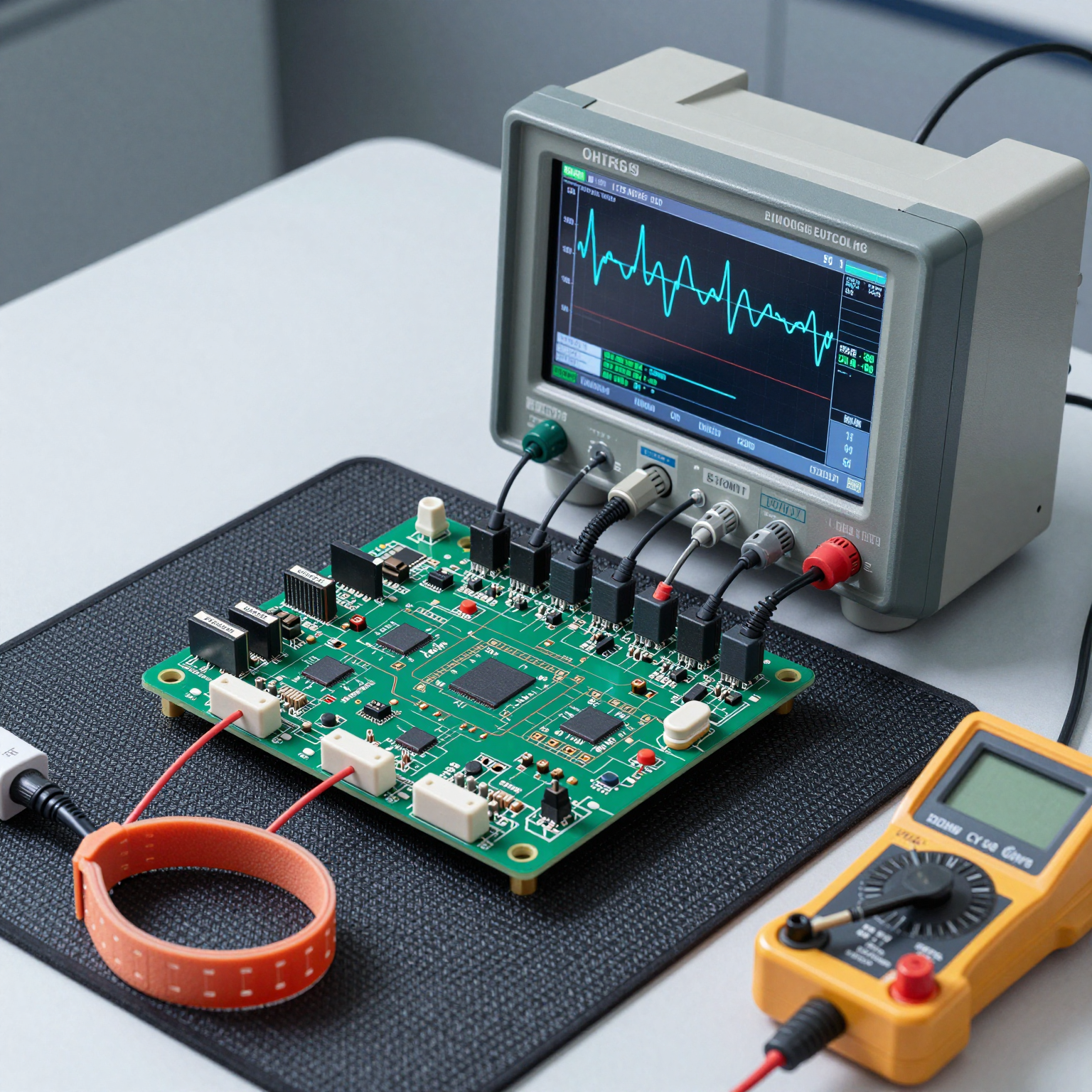
Step 6: Testing and Validation
No Prototype PCB Assembly is complete without thorough testing. Common evaluation methods include:
- Power-on tests
- In-circuit testing (ICT)
- Functional testing using custom jigs
- Environmental stress screening (optional)
Testing confirms that the board operates within specifications and identifies areas for improvement.
Benefits of Professional Prototype PCB Assembly Services
While some teams attempt DIY assembly, partnering with a professional PCB assembly manufacturer offers significant advantages:
Faster Time-to-Market
Experienced manufacturers have streamlined workflows, dedicated equipment, and strong supplier relationships. This translates into quicker turnaround times for PCB Sampling, accelerating your overall development cycle.
Higher Quality and Reliability
Professional facilities adhere to strict quality standards (e.g., IPC-A-610 Class 2/3), ensuring consistent results. Their expertise minimizes human error and improves first-pass yield.
Access to Advanced Technologies
From micro BGA packages to impedance-controlled layouts, professional assemblers handle complex designs that would be difficult or impossible to assemble manually.
For insight into handling challenging components, see our article on BGA assembly challenges.
Scalability
A good prototype partner can seamlessly transition your project from sampling to medium and high-volume production. This continuity eliminates the need to qualify a new vendor later.
Choosing the Right Partner for Your Prototype Needs
Selecting the right service provider is crucial. Here are key factors to consider:
Turnaround Time
Look for companies offering rapid prototyping options—some deliver assembled boards in 5–7 days or less.
Minimum Order Quantity (MOQ)
Ensure the manufacturer supports low MOQs suitable for PCB Sampling. Many accept orders as small as one unit.
Technical Capabilities
Verify that the assembler can handle your specific requirements:
- Fine-pitch components
- Mixed-technology boards
- Specialized finishes (e.g., immersion silver, OSP)
- Conformal coating or potting (if needed)
Explore detailed information about PCB manufacturing capabilities to ensure alignment with your needs.
Support and Communication
Responsive customer support and clear communication channels make the process smoother. Look for teams that assign dedicated project managers or technical liaisons.
If you're ready to move forward, don't hesitate to get a PCB quote and discuss your project requirements.
Common Challenges in Prototype PCB Assembly (And How to Avoid Them)
Despite best efforts, certain pitfalls can derail even well-planned prototyping efforts.
1. Incomplete or Inaccurate BOM
An incomplete Bill of Materials can delay component sourcing. Always double-check part numbers, values, tolerances, and package types.
Tip: Use standardized formats and include manufacturer-recommended alternatives where possible.
2. Poor Layout Practices
Crowded layouts, inadequate grounding, or improper decoupling can cause noise, overheating, or intermittent failures.
Solution: Follow best practices for PCB layout, including proper power distribution and signal routing. Refer to resources like the PCB surface finishes guide for optimal material selection.
3. Overlooking Test Points
Without accessible test points, debugging becomes extremely difficult. Design them into your board early.
4. Ignoring Thermal Management
High-power components generate heat. Ensure adequate copper pours, thermal vias, or heatsinks are included—even in prototypes.
Conclusion: Prototype Smart, Scale Confidently
Prototype PCB Assembly is far more than a preliminary step—it's a strategic investment in your product's success. By leveraging PCB Sampling effectively, you gain invaluable insights, reduce risk, and lay a solid foundation for scalable production.
Whether you're validating a new sensor module or refining a medical device, choosing the right partner makes all the difference. With access to advanced tools, expert engineering support, and end-to-end services—from design review to final testing—you can bring innovative ideas to life faster and more reliably.
Ready to turn your concept into reality? Connect with a trusted PCB assembly manufacturer today and start your journey from prototype to product.