
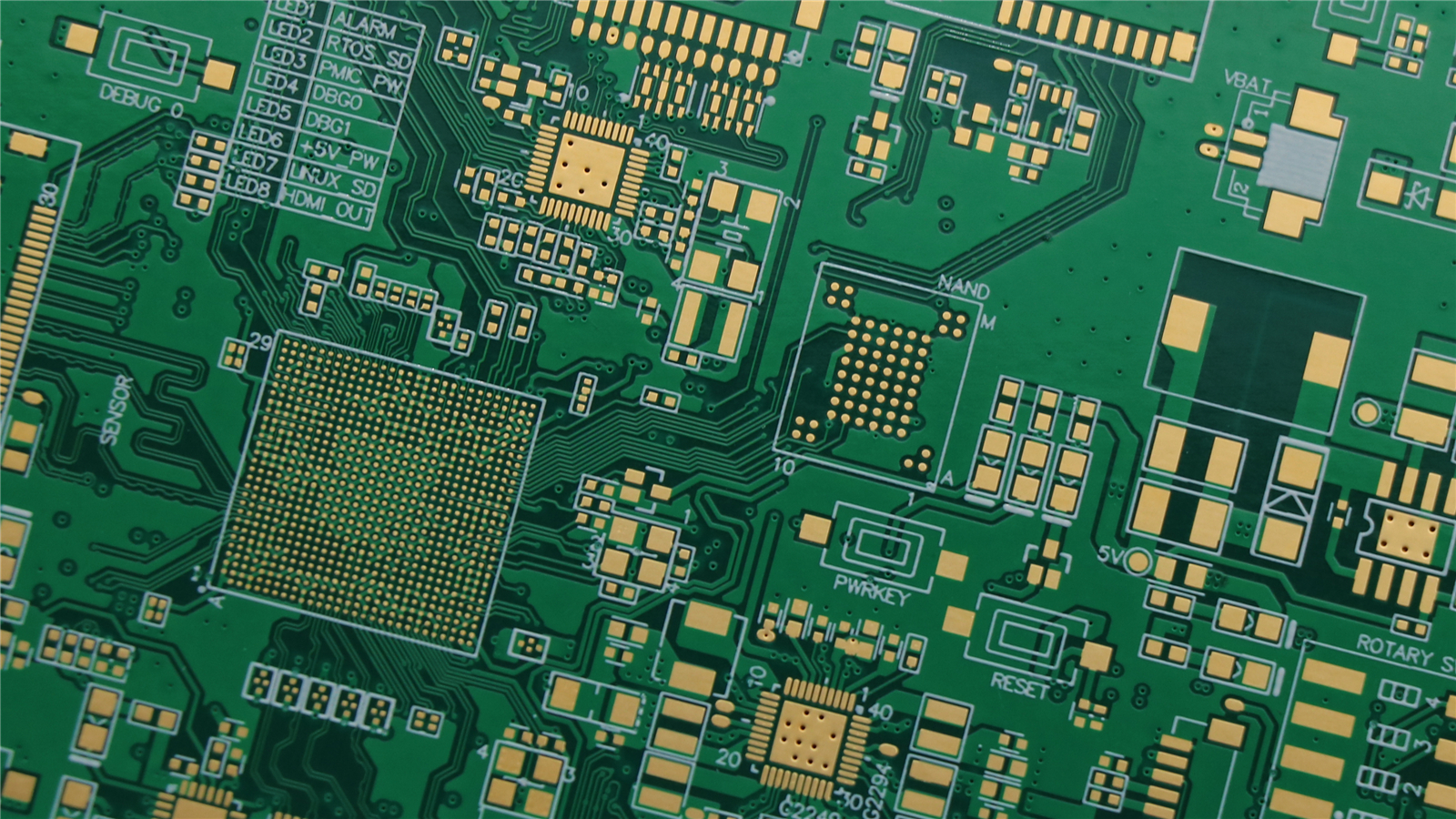
HDI基板
(76 reviews)
HDI基板
HDI基板
高度な電子機器向けのHigh Density Interconnect (HDI) 基板
Key Features
マイクロビア
レーザー加工ビア < 0.15mm
ファインライン
配線幅/間隔 < 0.075mm
高い信号品質
高速通信向けに最適化
コンパクト設計
より小さなスペースでより多くの機能
Specifications
| 層数 | 4-30層 |
| ビア技術 | ブラインド, ベリー, マイクロ |
| アスペクト比 | 最大 10:1 |
| 最小配線/間隔 | 0.05mm/0.05mm |
| 材料 | 高Tg FR4 |
エンジニアリング上の確認事項
見積り前の製造レビュー
HDI boards need fabrication and assembly decisions to stay linked. A realistic stackup and via strategy should be reviewed before the layout is frozen.
- Confirm layer count, microvia structure, sequential lamination, via-in-pad requirements, and the escape strategy around fine-pitch packages.
- Review stackup, impedance-sensitive layers, copper balance, registration, solder mask, and inspection access before release.
- Align the fabrication build with BGA assembly, X-ray or AOI coverage, test access, and the product reliability stage.