
Panduan Desain Titik Uji PCB: Cara Meningkatkan Akses ICT, Probe Terbang, dan Uji Fungsional
SUNTOP Electronics
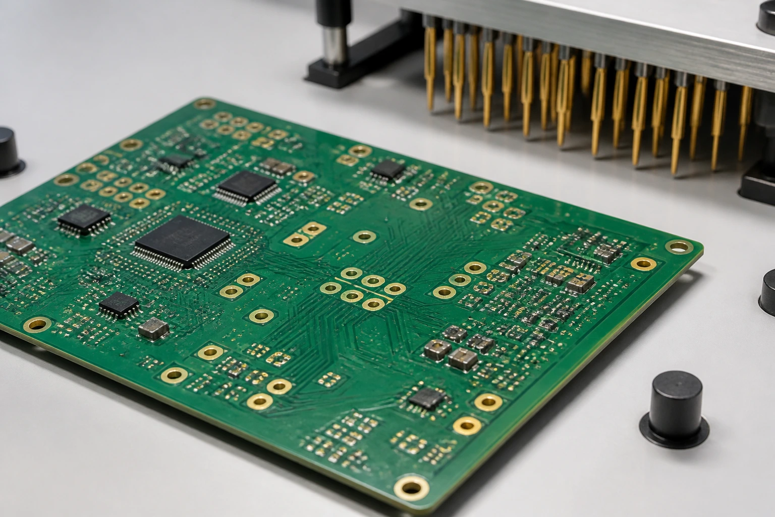
PCB test point design is one of the easiest things to postpone during layout and one of the most painful to fix after boards arrive for assembly. A board can be electrically correct and still be awkward to inspect, slow to debug, or difficult to validate if the team never planned clean access to key nets, rails, interfaces, and programming points.
That is why PCB test point design should be reviewed before fabrication or assembly release. Good test access helps engineering teams debug faster, helps contract manufacturers prepare realistic validation steps, and helps sourcing teams compare whether a supplier supports only assembly or also practical production test readiness.
In broader design for testing, the goal is to make verification practical during manufacturing. This guide explains what good test-point planning means in practice, where placement decisions matter most, and what to send a manufacturing partner before quote or build.
What PCB Test Point Design Means and Why It Matters
PCB test point design means planning accessible electrical contact locations so a board can be checked, programmed, debugged, or validated without guesswork. It is about making sure the points that matter are still reachable after assembly, panelization, and real handling constraints.
A useful access review asks practical questions such as:
- which rails, clocks, buses, reset lines, and interfaces may need access
- whether access is needed for ICT, flying probe, functional test, firmware loading, or debug
- whether probe contact will remain reliable after components, shields, connectors, or enclosures are added
- whether the chosen access points support repeatable testing instead of one-off bench probing
Where to Place PCB Test Points
The best test-point layout starts by deciding which nets truly need controlled access. Important power rails, reset paths, communication lines, programming interfaces, and high-risk analog nodes often do.

Clear spacing around test pads helps probes contact important nets more reliably during debug and production validation.
Placement quality depends on four things:
- Reachability: the probe or pogo pin must physically land without colliding with tall parts, connectors, heatsinks, or shielding.
- Stability: the board should not flex excessively or require awkward pressure to make contact.
- Clarity: teams should understand what each access point is for.
- Process fit: the access pattern should still work after solder mask, panel rails, depanelization, and assembly sequence.
If the board is headed into quality testing services, check test-point accessibility with assembly context in mind.
How Test Point Design Changes With ICT, Flying Probe, and Functional Test
Test-point planning should reflect the test method the program is likely to use.
For boards that may use in-circuit test, access needs to be more structured because dedicated fixtures depend on predictable contact locations. If the board may rely on a flying probe tester, the layout may tolerate more flexibility, but probe time, pad accessibility, and fixture assumptions still matter.
Functional validation adds another layer. The board may need power input, programming headers, communication ports, or controlled access to signals not in a classic ICT net list. The access plan should work together with connector planning and mechanical support, not as a separate checklist.
This is where teams should distinguish between prototype convenience and production discipline. A repeatable manufacturing flow usually needs clearer access logic that supports the PCB assembly service workflow without improvisation.
Mechanical and Documentation Details Teams Often Miss
Many access problems come from mechanical or documentation details never reviewed alongside the layout:
- test points placed too close to rails, tabs, or breakaway features
- access pads blocked by final enclosure assumptions or daughtercard stacking
- no clear note about which side of the board should be contacted
- reference naming or debug notes that exist in email but not in the release package
- fixture support needs ignored even though probe pressure may bend the board
Common Test Point Design Mistakes
The most common mistake is waiting until after layout release to ask what needs to be measured. Another is assuming debug pads are automatically good production-test pads. Teams also create problems when they add access points without clarifying purpose.
Good test-point planning is selective. It should support meaningful verification, not turn the layout into a field of pads that adds complexity without improving yield or debug speed.
How to Hand Off Test Point Intent to Your PCBA Partner
A manufacturer can only review test readiness clearly if the release package explains what the layout intends. A better handoff package includes:
- board revision and assembly files matching the intended test access
- notes on which nets, rails, or interfaces need reliable contact
- programming or debug expectations if firmware loading matters
- side-specific contact assumptions or fixture support concerns
- whether the board aims at ICT, flying probe, functional validation, or a staged combination
- areas where the supplier should suggest better access before build
When those details are shared early, the supplier can comment on whether the current test point design is strong enough before the first build starts. If you want that review, the cleanest next step is a short discussion through the contact page.
FAQ About PCB Test Point Design
Does every PCB need dedicated test points?
No. The right level of access depends on product complexity, debug risk, production volume, and the planned test method. The goal is useful, reachable access where it actually supports verification.
Should PCB test point design be handled by layout only?
No. Layout owns placement, but effective planning usually needs input from hardware, test, manufacturing, and sourcing teams.
When should a manufacturer review PCB test point design?
Ideally before fabrication or assembly release, especially if the board may need ICT, flying probe, programming support, or repeatable functional validation. Early review is cheaper than adding awkward fixes after the first build.
Conclusion
Test-point planning is a small layout decision area with a large effect on debug speed, fixture practicality, and production readiness. When teams decide early what needs access, keep those points reachable through assembly reality, and explain the intent clearly to a manufacturing partner, they reduce avoidable delay between first layout and reliable board validation.