
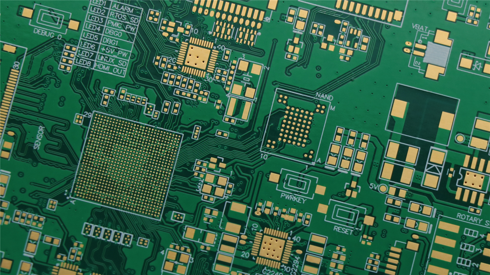
HDI PCB
(76 reviews)
HDI PCB
HDI PCB
لوحات دوائر مطبوعة ذات كثافة توصيل عالية للأجهزة الإلكترونية المتقدمة
Key Features
Micro Vias
فتحات محفورة بالليزر < 0.15mm
خطوط دقيقة
مسار/فراغ < 0.075mm
سلامة إشارة عالية
محسن للسرعة العالية
تصميم مدمج
وظائف أكثر في مساحة أقل
Specifications
| عدد الطبقات | 4-30 طبقة |
| تقنية الفتحات | عمياء, مدفونة, دقيقة |
| نسبة الارتفاع | حتى 10:1 |
| أقل مسار/فراغ | 0.05mm/0.05mm |
| المادة | High Tg FR4 |
Engineering considerations
Manufacturing review before quote
HDI boards need fabrication and assembly decisions to stay linked. A realistic stackup and via strategy should be reviewed before the layout is frozen.
- Confirm layer count, microvia structure, sequential lamination, via-in-pad requirements, and the escape strategy around fine-pitch packages.
- Review stackup, impedance-sensitive layers, copper balance, registration, solder mask, and inspection access before release.
- Align the fabrication build with BGA assembly, X-ray or AOI coverage, test access, and the product reliability stage.