
Stackup feasibility
Review layer roles, reference planes, dielectric spacing, finished thickness, copper distribution, and practical material options before routing is frozen.
Signal integrity manufacturing
Turn impedance targets into a stackup and fabrication package that your supplier can quote, build, and verify without guessing.
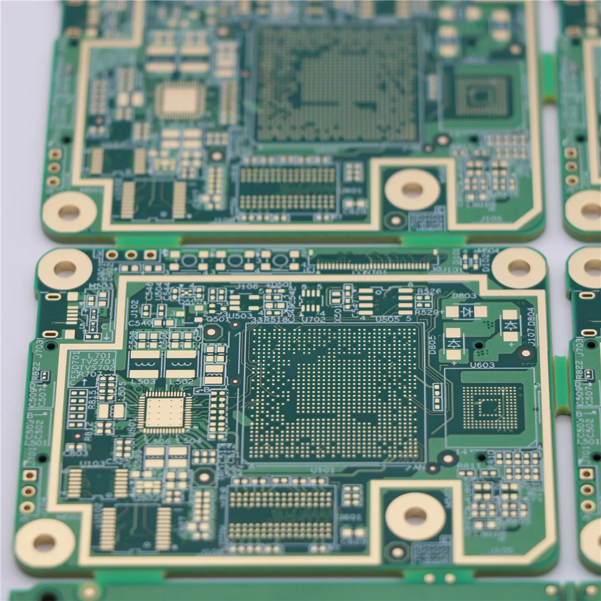
From target to build
Stackup assumptions, routing geometry, material data, and validation requirements stay connected from design review through production.
What we review
A calculator can show whether a geometry is directionally plausible. A production-ready board also needs a real laminate build, copper model, reference-plane plan, process window, and clear acceptance criteria. We review those inputs early so routing, quoting, fabrication, and testing are working from the same intent.
Use the level of review that matches your board risk, from an early stackup discussion to a production-intent validation build.
Review layer roles, reference planes, dielectric spacing, finished thickness, copper distribution, and practical material options before routing is frozen.
Coordinate single-ended and differential targets with trace width, spacing, copper thickness, layer assignment, escape routing, and process margin.
Compare FR4, low-loss, or hybrid options using frequency, Dk, Df, copper profile, availability, loss budget, and sourcing risk rather than brand names alone.
Define coupon expectations, TDR or network-analysis needs, report fields, and the feedback loop needed to keep the released build traceable.
The exact sequence depends on the project, but these checkpoints keep electrical intent and manufacturing reality aligned.
Identify target nets, interfaces, layers, frequency range, board thickness, and fixed versus adjustable requirements.
Compare dielectric, copper, reference-plane, and geometry assumptions with the intended fabrication process.
Send the manufacturer a readable release package instead of relying on Gerbers or scattered email notes.
Confirm whether the order needs a representative coupon, a defined test method, or a production-intent validation build.
Review measured results and any stackup adjustment against the same revision and acceptance criteria.
Give engineering and purchasing enough detail to review the job without reverse-engineering your design intent.
Testing is most useful when the measurement method and acceptance criteria are agreed before the board is built.
Calculator results and reference charts are early engineering estimates. Final values depend on the actual laminate combination, copper profile, fabrication tolerances, and agreed test method.
Not reliably. Gerbers show geometry but do not fully define the laminate build, copper condition, reference-plane relationship, material data, or acceptance method. Those inputs must be reviewed together.
No. A well-characterized FR4 build can be suitable for many boards. Low-loss or hybrid materials deserve review when frequency, channel length, insertion loss, phase stability, or tolerance requirements make standard assumptions too narrow.
Before routing and fabrication files are fully frozen whenever stackup, thickness, copper, or impedance constraints can change the layout. Early review leaves more room for a practical build option.
Send the target values, current stackup direction, board stage, and known constraints. We can help turn the early assumptions into a clearer manufacturing review package.