
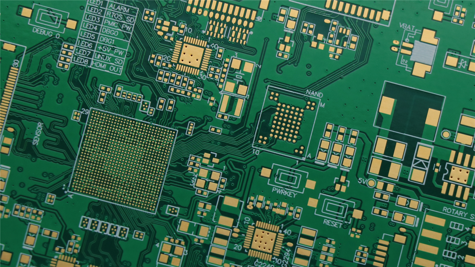
PCB HDI
(76 recenzii)
PCB HDI
PCB HDI
PCB-uri cu interconectare de înaltă densitate pentru dispozitive electronice avansate
Caracteristici cheie
Micro Vias
Vias găurite cu laser < 0.15mm
Linii Fine
Traseu/Spațiu < 0.075mm
Integritate Semnal Ridicată
Optimizat pentru viteză mare
Design Compact
Mai multă funcționalitate în mai puțin spațiu
Specificații
| Număr straturi | 4-30 straturi |
| Tehnologie Via | Orb, Îngropat, Micro |
| Raport de Aspect | Până la 10:1 |
| Min Traseu/Spațiu | 0.05mm/0.05mm |
| Material | High Tg FR4 |
Engineering considerations
Manufacturing review before quote
HDI boards need fabrication and assembly decisions to stay linked. A realistic stackup and via strategy should be reviewed before the layout is frozen.
- Confirm layer count, microvia structure, sequential lamination, via-in-pad requirements, and the escape strategy around fine-pitch packages.
- Review stackup, impedance-sensitive layers, copper balance, registration, solder mask, and inspection access before release.
- Align the fabrication build with BGA assembly, X-ray or AOI coverage, test access, and the product reliability stage.