
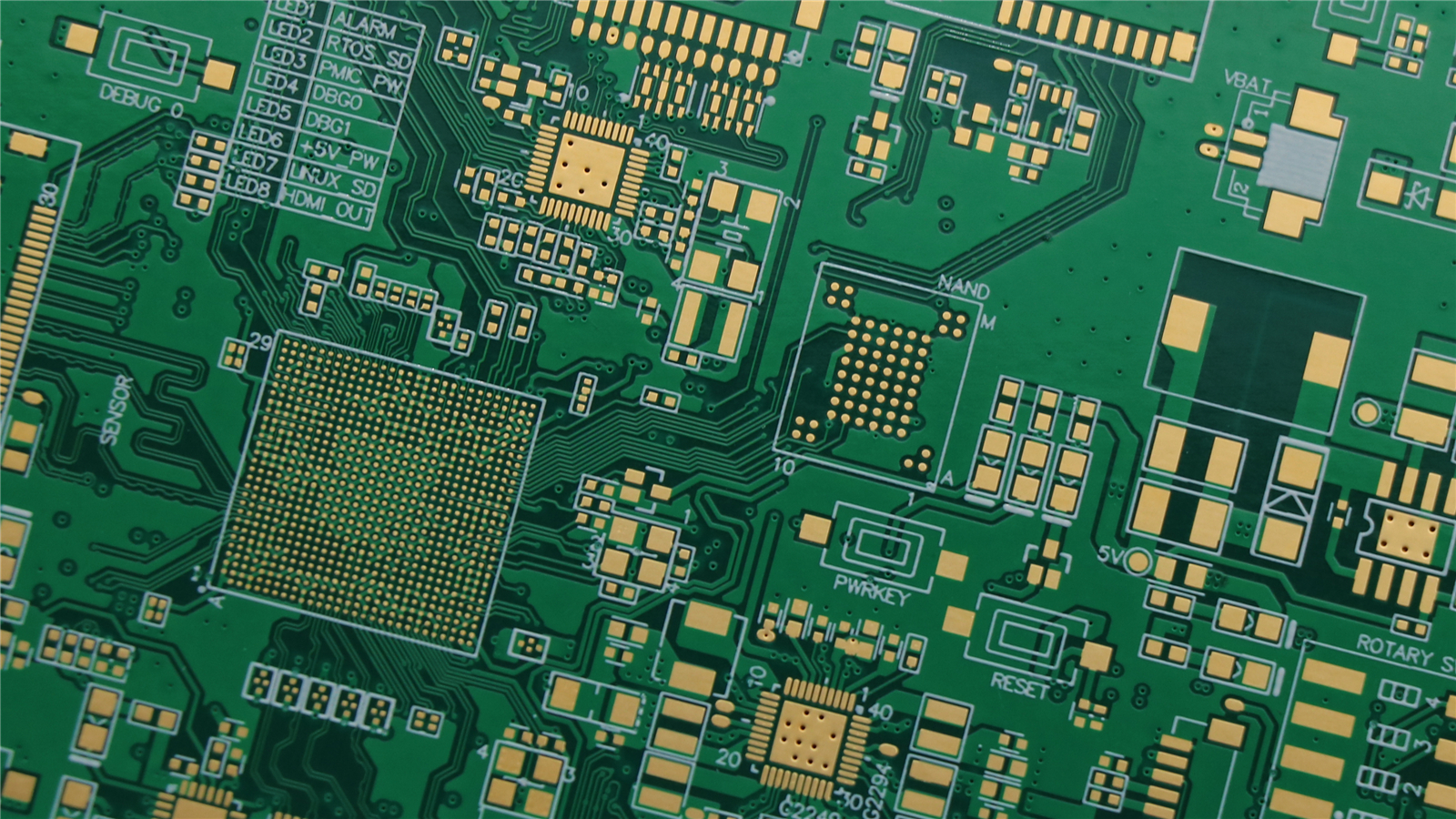
PCB HDI
(76 avis)
PCB HDI
PCB HDI
PCB à Interconnexion Haute Densité pour appareils électroniques avancés
Points forts
Micro Vias
Vias percés au laser < 0.15mm
Lignes Fines
Piste/Espace < 0.075mm
Haute Intégrité du Signal
Optimisé pour haute vitesse
Design Compact
Plus de fonctionnalités dans moins d'espace
Spécifications
| Nombre de couches | 4-30 couches |
| Technologie Via | Borgne, Enterré, Micro |
| Ratio d'Aspect | Jusqu'à 10:1 |
| Min Piste/Espace | 0.05mm/0.05mm |
| Matériau | Haut Tg FR4 |
Considérations d’ingénierie
Revue de fabrication avant devis
HDI boards need fabrication and assembly decisions to stay linked. A realistic stackup and via strategy should be reviewed before the layout is frozen.
- Confirm layer count, microvia structure, sequential lamination, via-in-pad requirements, and the escape strategy around fine-pitch packages.
- Review stackup, impedance-sensitive layers, copper balance, registration, solder mask, and inspection access before release.
- Align the fabrication build with BGA assembly, X-ray or AOI coverage, test access, and the product reliability stage.