The Future of HDI PCB Technology: Trends and Innovations
Rachel Rossannie
As we approach forward, the electronics industry is undergoing a transformation driven by the relentless demand for smaller, faster, and more efficient devices. At the heart of this evolution lies High-Density Interconnect (HDI) PCB technology—a critical enabler of next-generation electronic products across consumer, medical, automotive, and industrial sectors. As a leading PCB manufacturing services provider, SUNTOP Electronics is at the forefront of advancing HDI PCB capabilities to meet tomorrow’s challenges today.
This comprehensive analysis explores the key trends, technological breakthroughs, and market dynamics shaping the future of HDI PCBs. From miniaturization and flexible substrates to advanced materials and intelligent manufacturing, we’ll examine how innovation is redefining what’s possible—and how our expertise in HDI Manufacturing, HDI Assembly, and rapid prototyping positions us as a trusted partner for cutting-edge electronics development.
What Is HDI PCB Technology?
High-Density Interconnect (HDI) PCBs are printed circuit boards designed with finer trace widths, tighter spacing, higher layer counts, and microvias to achieve greater component density and improved electrical performance compared to traditional PCBs. These boards enable complex circuitry in compact spaces, making them ideal for smartphones, wearables, IoT sensors, medical implants, and high-speed communication systems.
Unlike standard multilayer PCBs that use through-hole vias, HDI designs utilize blind, buried, and stacked microvias—often laser-drilled—to connect layers efficiently without consuming valuable surface real estate. This allows designers to place components closer together, reduce signal path lengths, minimize electromagnetic interference (EMI), and enhance overall system reliability.
SUNTOP Electronics specializes in producing high-reliability HDI PCBs tailored for demanding applications. Whether you need an HDI Sample for initial testing or full-scale production runs, our state-of-the-art fabrication lines ensure precision, consistency, and compliance with IPC Class 3 standards.
Key Drivers Behind the Growth of HDI PCBs
Several macroeconomic and technological forces are accelerating the adoption of HDI PCBs globally:
Miniaturization of Consumer Electronics
Smartphones, tablets, smartwatches, and wireless earbuds continue to shrink in size while increasing functionality. Consumers expect powerful processors, multiple cameras, long battery life, and seamless connectivity—all packed into sleek form factors. HDI PCBs make this possible by enabling dense routing and component placement on limited board space.
For example, Apple's iPhone series has relied heavily on HDI architecture since the iPhone 4, using sequential lamination and microvia stacking to support its A-series chips and advanced camera modules. As 5G modems, AI accelerators, and augmented reality features become standard, the need for even denser interconnect solutions will grow.
Expansion of IoT and Edge Computing
The Internet of Things (IoT) ecosystem now spans billions of connected devices—from home automation hubs to industrial monitoring systems. Many of these operate at the edge, requiring local processing power and low-latency communication. HDI PCBs allow manufacturers to integrate powerful SoCs (System-on-Chips), memory, RF transceivers, and sensors onto small, energy-efficient boards.
Moreover, ruggedized HDI designs are being deployed in harsh environments such as oil rigs, agricultural fields, and smart city infrastructure. These require enhanced durability, thermal management, and resistance to moisture and vibration—all achievable through optimized HDI layouts and material selection.
Advancements in Automotive Electronics
Modern vehicles are essentially computers on wheels. Advanced Driver Assistance Systems (ADAS), infotainment units, electric vehicle (EV) battery management systems, and autonomous driving platforms rely on sophisticated electronics that demand high-speed signaling and fault tolerance.
HDI PCBs play a vital role in automotive radar modules, LiDAR sensors, and domain controllers where space constraints and EMI sensitivity are major concerns. With ISO/TS 16949-certified processes and rigorous testing protocols, SUNTOP Electronics supports Tier 1 suppliers and OEMs in delivering reliable HDI FPC and rigid-flex solutions for mission-critical applications.
Medical Device Innovation
In healthcare, wearable monitors, implantable devices, and portable diagnostic tools are transforming patient care. These devices must be lightweight, biocompatible, and capable of continuous operation—requirements perfectly suited to HDI technology.
Flexible and stretchable HDI substrates enable conformal circuits that can bend around organs or fit inside hearing aids and insulin pumps. Our experience in HDI prototype development ensures fast turnaround times for medical startups and established device makers alike, helping bring life-saving technologies to market faster.
Emerging Trends Shaping HDI PCB Development
Looking ahead, several emerging trends are set to redefine HDI PCB design, manufacturing, and application. Let’s explore the most impactful ones.
1. Ultra-Fine Line Widths
and Microvia Scaling
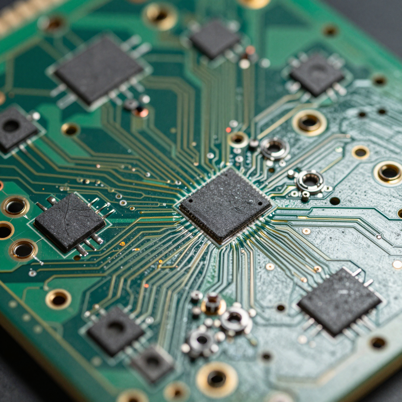
One of the defining characteristics of next-gen HDI PCBs is the push toward ultra-fine line/space dimensions—below 30µm (1.2 mil). Achieving such precision requires advanced photolithography equipment, specialized resins, and controlled impedance techniques.
At SUNTOP Electronics, we have invested in semi-additive processing (SAP) and modified semi-additive processing (mSAP) technologies, which allow us to produce traces as narrow as 20µm with consistent quality. These methods involve depositing thin copper layers and selectively etching away unwanted material, resulting in sharper definition and reduced signal loss.
Coupled with smaller microvias (down to 40µm diameter), these advancements enable higher I/O density for BGAs and chip-scale packages (CSPs). For customers developing AI chips, FPGA-based accelerators, or millimeter-wave modules, this level of detail is essential for maintaining signal integrity at multi-gigabit speeds.
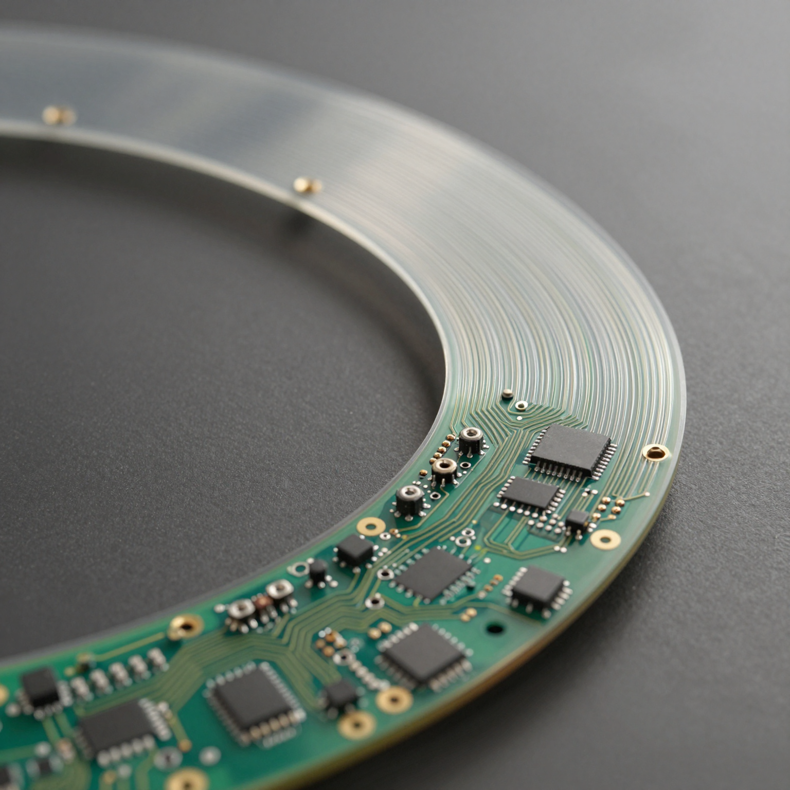
2. Rise of HDI Flexible and Rigid-Flex Circuits
While rigid HDI PCBs dominate mobile computing, the demand for HDI FPC (Flexible Printed Circuits) is growing rapidly due to their ability to conform to 3D shapes, reduce weight, and eliminate connectors.
Applications like foldable smartphones, AR/VR headsets, robotic end-effectors, and minimally invasive surgical tools benefit from flexible HDI substrates that combine dynamic bending capability with high-speed performance. Polyimide films remain the material of choice, but newer alternatives like liquid crystal polymer (LCP) offer superior RF properties and lower moisture absorption.
Rigid-flex HDI boards merge the best of both worlds—providing mechanical stability in certain areas while allowing flexibility elsewhere. They simplify assembly by replacing cables and connectors, improve reliability by reducing solder joints, and save space in densely packed enclosures.
Our team excels in designing and fabricating complex rigid-flex HDI stacks with precise alignment, via filling, and coverlay registration. Whether it's a two-layer flex or an eight-layer rigid-flex hybrid, we deliver robust solutions backed by extensive PCB quality testing and validation procedures.
3. Adoption of Embedded Components and Active Substrates
To further increase integration density, some designers are moving beyond surface-mount components and embedding passive and active elements directly within the PCB layers.
Embedded resistors, capacitors, and even ICs can be integrated during the lamination process, freeing up surface area for other components and shortening interconnect paths. This not only improves electrical performance but also enhances thermal dissipation and shock resistance.
While still niche due to cost and complexity, embedded technology is gaining traction in aerospace, defense, and high-performance computing. In 2026, we anticipate wider adoption as manufacturing yields improve and design tools mature.
SUNTOP Electronics offers pilot programs for HDI prototype builds featuring embedded passives, supporting clients who want to evaluate this technology before scaling up. Our engineers work closely with design teams to optimize stack-up configurations, select appropriate dielectrics, and ensure manufacturability.
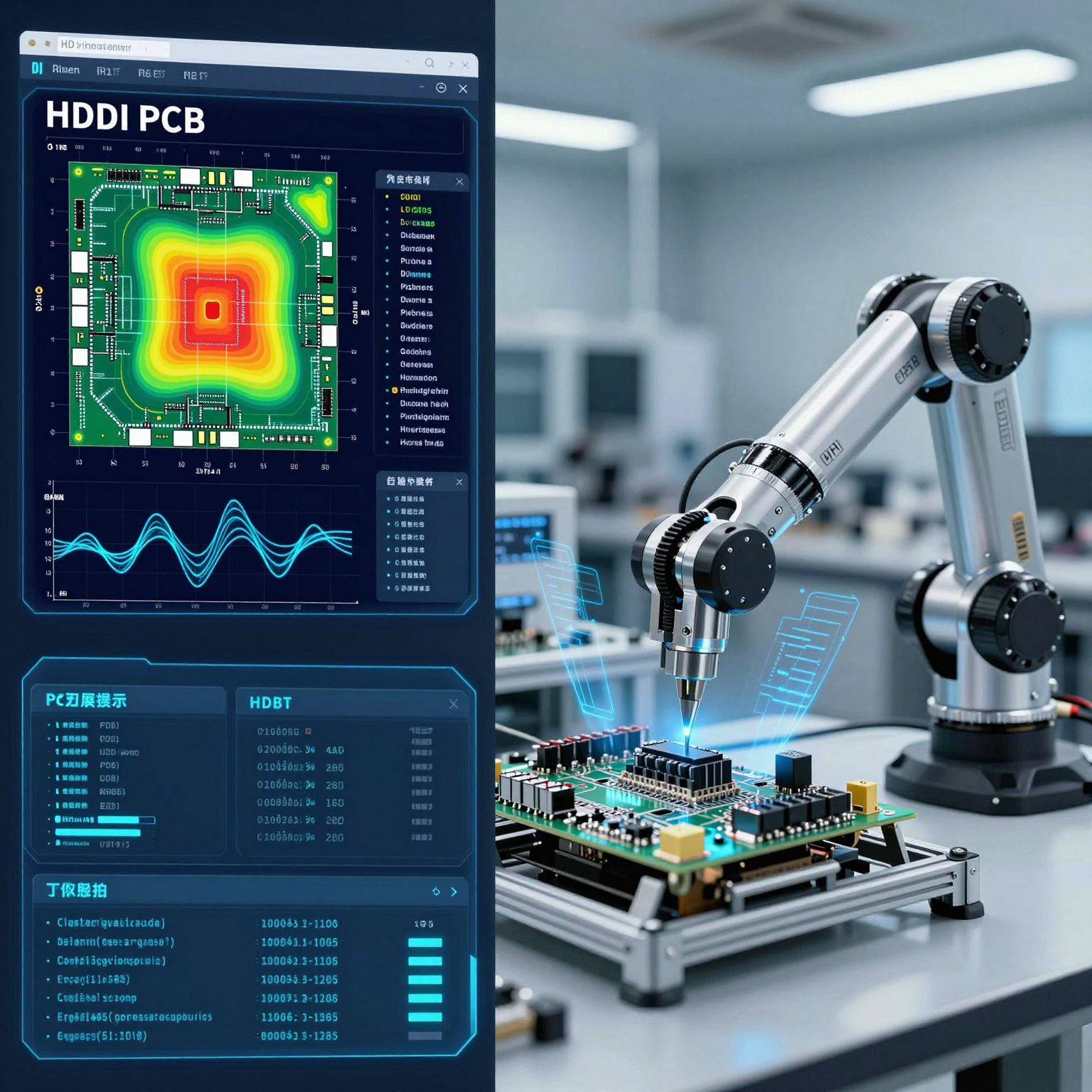
4. Integration of AI and Machine Learning in Design and Inspection
Artificial intelligence (AI) is beginning to transform every stage of the HDI PCB lifecycle—from layout optimization to automated optical inspection (AOI).
During the design phase, AI-powered tools can analyze schematics and suggest optimal routing strategies, identify potential crosstalk zones, and predict thermal hotspots. This reduces iteration cycles and helps avoid costly redesigns later.
On the factory floor, machine learning algorithms enhance AOI systems by distinguishing between true defects and harmless anomalies with higher accuracy than traditional rule-based systems. Deep learning models trained on thousands of images can detect subtle issues like microvia voids, delamination, or plating irregularities that human inspectors might miss.
We’ve integrated AI-driven analytics into our 6-step quality control process, significantly improving first-pass yield rates and reducing false callbacks. This translates into faster delivery times and lower costs for our customers.
Additionally, predictive maintenance powered by AI helps monitor equipment health in real time, preventing unplanned downtime and ensuring consistent output quality across large production batches.
5. Sustainable Materials and Green Manufacturing Practices
Environmental sustainability is no longer optional—it’s a business imperative. Regulatory bodies like the EU’s RoHS and REACH directives, along with corporate ESG goals, are pushing electronics manufacturers to adopt greener practices.
In response, HDI PCB producers are exploring halogen-free laminates, lead-free surface finishes, water-based cleaning agents, and recyclable packaging. Some are experimenting with bio-based resins derived from renewable sources, though widespread adoption awaits improvements in performance and cost parity.
SUNTOP Electronics is committed to minimizing our environmental footprint. We use energy-efficient machinery, implement closed-loop water recycling in our plating lines, and partner with suppliers who share our sustainability values. Our facilities comply with ISO 14001 environmental management standards, and we continuously audit our supply chain for responsible sourcing.
Customers seeking eco-friendly HDI Manufacturing options can collaborate with us to specify green materials and processes without compromising performance or reliability.
6. Increased Use of mmWave and High-Speed Digital Interfaces
With the rollout of 5G, Wi-Fi 6E/7, and upcoming 6G research, HDI PCBs must handle signals in the millimeter-wave (mmWave) spectrum—ranging from 24GHz to over 100GHz.
These frequencies are highly susceptible to losses caused by conductor roughness, dielectric absorption, and impedance mismatches. Therefore, next-gen HDI boards require ultra-smooth copper foils, low-Dk/Df laminates (such as Panasonic Megtron 7 or Nelco N4000-13SI), and precise controlled impedance design.
Furthermore, high-speed serial interfaces like PCIe Gen 6 (64 GT/s), USB4 v2.0 (80 Gbps), and Thunderbolt 5 demand strict differential pair routing, length matching, and shielding techniques—all made feasible through HDI’s fine-feature capabilities.
Our engineering team employs advanced simulation software to model signal behavior and validate designs pre-fabrication. Combined with impedance-controlled manufacturing and post-production TDR (Time Domain Reflectometry) testing, we ensure your high-speed HDI boards perform flawlessly in real-world conditions.
How SUNTOP Electronics Supports HDI Innovation
As a vertically integrated PCB assembly manufacturer, SUNTOP Electronics provides end-to-end solutions—from concept to mass production—for companies leveraging HDI technology. Here’s how we stand out:
Rapid Prototyping and Low-Volume Production
Speed is crucial in product development. That’s why we offer accelerated HDI prototype services with turnkey support, including electronic component sourcing, quick-turn fabrication, and functional testing.
Whether you're validating a new smartphone module or iterating on a medical sensor design, our streamlined workflow delivers HDI Sample boards in as little as 5–7 days. We support various build types, including single-sided, double-sided, and multi-layer HDI with staggered or stacked microvias.
Our online portal allows customers to upload Gerber files, receive instant DFM feedback, and request a quote seamlessly. For those unfamiliar with the process, our blog post on the complete guide to PCB assembly offers valuable insights into each step.
Advanced HDI Manufacturing Capabilities
Our production facilities feature:
- Laser drilling machines capable of creating microvias down to 40µm
- Precision imaging systems with ±10µm alignment accuracy
- Sequential lamination presses for complex build-ups
- mSAP lines for ultra-fine line width patterning
- Automated plating and etching stations with real-time monitoring
We support a wide range of materials, including FR-4 High-Tg, Rogers, Arlon, Isola, and specialty flex films. Surface finishes include ENIG, ENEPIG, Immersion Silver, OSP, and hard gold for edge connectors.
All processes adhere to IPC-A-600H and IPC-6012 Class 3 standards, ensuring maximum reliability for commercial and industrial applications.
For detailed information about our technical limits and supported technologies, visit our PCB manufacturing capabilities page.
Expertise in HDI Assembly and Complex SMT Processes
Fabricating an HDI PCB is only half the battle—populating it with components presents its own set of challenges. Fine-pitch BGAs, 01005 passives, wafer-level CSPs, and PoP (Package-on-Package) assemblies require precision placement, uniform reflow profiles, and thorough post-solder inspection.
Our SMT lines are equipped with:
- High-resolution pick-and-place machines with vision alignment down to 15µm
- Nitrogen-reflow ovens for void reduction in BGA joints
- AXI (Automated X-ray Inspection) for hidden joint verification
- Flying probe and ICT testers for electrical validation
We specialize in HDI Assembly for high-mix, low-volume projects as well as dedicated lines for high-volume production. Our experience with BGA assembly challenges ensures minimal defects and excellent yield rates—even for packages with pitches below 0.4mm.
In addition, we provide conformal coating, potting, and mechanical boxing services upon request, offering a truly turnkey solution.
Comprehensive Quality Assurance and Testing
Quality isn’t an afterthought—it’s built into every stage of our operations. Our 6-step quality control process includes:
- Incoming material inspection
- Pre-lamination QA checks
- In-process AOI and X-ray
- Final electrical testing (continuity, isolation)
- Functional testing (customer-specific)
- Packaging and shipment verification
Each board undergoes rigorous testing to ensure compliance with specifications. We also offer third-party certification support for industries requiring UL, CE, or FCC approvals.
Learn more about our approach in our article on the PCB quality control process.
Customer-Centric Support and Global Reach
From initial consultation to after-sales service, we prioritize clear communication, transparency, and responsiveness. Our project managers act as single points of contact, providing regular updates and addressing concerns promptly.
We serve clients across North America, Europe, Asia, and Australia, shipping worldwide with reliable logistics partners. Whether you’re a startup in Silicon Valley or an enterprise in Germany, we adapt to your timeline, language, and regulatory needs.
Interested in partnering with us? Contact a PCB manufacturer today to discuss your next HDI project.
Industry Applications Driving HDI Demand in 2026
Understanding where HDI technology is being applied helps contextualize its importance. Below are key sectors expected to drive growth through 2026.
1. 5G Infrastructure and Mobile Devices
Base stations, small cells, and user equipment all rely on HDI PCBs to manage massive MIMO antenna arrays, RF front-ends, and baseband processing units. The shift to mmWave frequencies demands tighter integration and better thermal management—both strengths of HDI design.
Mobile phones, especially flagship models, will continue to incorporate more sensors, larger batteries, and advanced displays—all within constrained footprints. HDI enables the necessary miniaturization while supporting faster data transfer and longer battery life.
2. Wearable and Implantable Medical Devices
Fitness trackers, glucose monitors, neurostimulators, and pacemakers require ultra-compact, biocompatible circuits. HDI FPC solutions allow these devices to be lightweight, flexible, and durable enough for long-term use.
With aging populations and rising chronic disease rates, the global wearable medical device market is projected to exceed $100 billion by 2026. This creates immense opportunities for innovators—and for manufacturers like SUNTOP Electronics who can deliver reliable, certified products.
3. Electric and Autonomous Vehicles
EVs generate significant heat and electromagnetic noise, necessitating robust PCB designs. Battery Management Systems (BMS), motor controllers, and charging modules all benefit from HDI’s superior thermal conductivity and EMI shielding.
Autonomous vehicles depend on sensor fusion—combining inputs from cameras, radar, LiDAR, and ultrasonic sensors. Each sensor module contains HDI boards that process data in real time. Reliability is paramount; a single failure could compromise safety.
We support automotive clients with AEC-Q200 qualified components, underfilling for thermal cycling resilience, and rigorous environmental stress screening.
4. Industrial Automation and Robotics
Smart factories rely on interconnected machines, programmable logic controllers (PLCs), and robotic arms—all powered by compact, high-performance controllers. HDI PCBs enable modular, scalable designs that can be upgraded easily.
Collaborative robots (cobots), in particular, require lightweight, responsive electronics that can operate safely alongside humans. Flexible HDI substrates allow wiring to be embedded directly into joints and limbs, reducing bulk and improving dexterity.
5. Aerospace and Defense
Military and aerospace systems demand extreme reliability under harsh conditions. Avionics, satellite communications, radar systems, and electronic warfare suites often use HDI PCBs for their size, weight, and power (SWaP) advantages.
With increased focus on hypersonic vehicles, drone swarms, and secure communications, the need for radiation-hardened, tamper-resistant HDI solutions will grow. While production volumes may be low, the technical requirements are among the highest in the industry.
Challenges Facing HDI PCB Manufacturers
Despite the promising outlook, HDI PCB development faces several hurdles that manufacturers must navigate:
1. Rising Material and Equipment Costs
Advanced laminates, ultra-low-loss dielectrics, and laser drilling systems come at a premium. Inflationary pressures and supply chain volatility have exacerbated cost increases, squeezing margins for fabricators.
SUNTOP Electronics mitigates this by maintaining strategic inventory buffers, negotiating long-term supplier contracts, and optimizing material utilization through nesting algorithms and panelization strategies.
2. Skilled Labor Shortage
Designing and manufacturing HDI PCBs requires deep expertise in high-speed layout, thermal modeling, and advanced processes like mSAP. There’s a global shortage of experienced engineers and technicians, particularly in regions with booming electronics markets.
To address this, we invest in training programs, collaborate with technical universities, and leverage digital twins and simulation tools to reduce reliance on manual troubleshooting.
3. Thermal Management at High Densities
Packing more components into smaller areas generates more heat. Without proper thermal pathways, performance degrades and lifespan shortens.
We employ thermal vias, metal cores, heat spreaders, and selective thick copper layers to dissipate heat effectively. Simulation tools help predict temperature distribution and guide design modifications early in the cycle.
4. Supply Chain Resilience
Recent disruptions—from pandemics to geopolitical tensions—have highlighted vulnerabilities in global supply chains. Single-source dependencies for critical materials or components pose risks.
Our strategy includes dual-sourcing key materials, qualifying alternate suppliers, and maintaining buffer stocks for high-risk items. We also offer electronic component sourcing services to help customers overcome shortages and obsolescence issues.
Conclusion: Partnering for Success in the HDI Era
As we look toward, HDI PCB technology will remain a cornerstone of innovation across virtually every electronics-driven industry. Its ability to enable smaller, smarter, and more connected devices makes it indispensable in the modern world.
At SUNTOP Electronics, we are not just observers of this trend—we are active participants shaping its trajectory. Through continuous investment in R&D, automation, and talent development, we empower innovators to turn bold ideas into reality.
Whether you need a single HDI prototype, a batch of HDI Sample units for field trials, or full-scale HDI Manufacturing and HDI Assembly services, we’re here to help. Our commitment to quality, speed, and customer satisfaction sets us apart in a competitive landscape.
Ready to take your next project to the next level? Get a PCB quote today and discover how SUNTOP Electronics can accelerate your path to market.