
How a PCBA Manufacturing Partner Reduces Design Iterations and Controls Quality Risk
SUNTOP Electronics
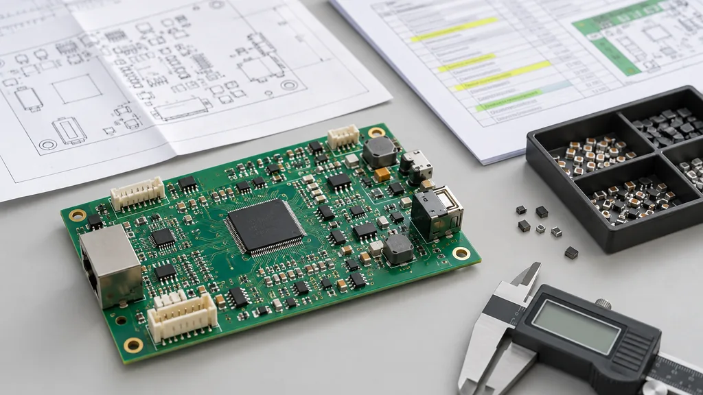
Hardware programs rarely slip because a board cost two dollars too much. They slip because the design needed a fourth spin, because a component went obsolete after layout was frozen, or because the first build arrived without test access and could not be validated without rework.
All of those events appear on the schedule as extra design iterations. Each iteration is a complete loop: change the design, re-fabricate, re-assemble, re-test, re-qualify. That loop, not the unit price, is what consumes engineering hours and calendar weeks.
This guide is about how a PCBA manufacturing partner affects that loop count. It covers where iterations actually come from, which ones a strong partner can remove, which ones it cannot, and how to tell the difference before you commit to a supplier.
Why iteration count, not unit price, decides your program schedule
A quote comparison optimises the wrong variable. A forty-cent difference per board on a five-hundred-board run is two hundred dollars. One avoidable spin costs weeks of engineering time, new stencils, a procurement reset, fixture and test-program changes, re-qualification, and a slip in the market window.
The industry rule of thumb is that the cost of correcting an issue grows by roughly an order of magnitude at each phase transition: design to prototype, prototype to production, production to field. That heuristic is not a precise accounting model, but it captures the direction correctly. A footprint error caught in review costs an email. The same error caught after assembly costs a rework order. Caught after shipment, it costs a recall.
So the question you are really asking a PCBA manufacturing partner is not "who is cheapest per board" but "who makes each loop shorter, and who prevents the loops that should never happen". Price still matters, but on any program with schedule risk it is a second-order variable next to loop count.
Where extra design iterations actually come from
In practice, most avoidable spins trace back to five sources. None of them are exotic process failures, none of them are caught by a quote, and all five are visible to a PCBA manufacturing partner before tooling is cut.
Ambiguous design intent
Do-not-populate parts marked only in a spreadsheet. Tolerances that are implied but never stated. Silkscreen notes that contradict the BOM. Alternate parts listed without the conditions under which they are acceptable.
The factory then has two options: guess, or stop and ask. Guessing produces a rework or a spin. Asking produces a delay. Both are avoidable at the design stage.
Manufacturing assumptions that were never verified
A footprint drawn to a nominal package while the actual supplier part has a different body size or lead form. Via-in-pad without fill and planarisation, which traps voids under a BGA. Thermal relief and copper balance that cause tombstoning or warpage at reflow. A panel layout that ignores assembly rails and fiducials, which then costs placement accuracy and handling.
Every one of these is checkable before tooling is cut, but only if someone who owns the process actually checks it. A quote does not check it.
Test access designed after the fact
No test points, no probe keep-outs, no functional test connector, no defined pass/fail criteria. The board then needs a spin purely to become testable, which is an iteration that adds no product value at all.
Component decisions made after layout freeze
Lifecycle status verified when the BOM was created but not re-checked at release. Minimum order quantities and packaging that force a different package. A substitute that needs a different land pattern. Sourcing surprises land as late engineering change orders, and late ECOs are the most expensive kind.
A handoff package that forces questions
A missing stackup and impedance target. No pick-and-place file with rotations. No assembly drawing. No statement of volume or delivery expectation. Every missing item becomes an email round trip. Multiply that by fifteen items and a week has disappeared before the first board is even produced.
What a PCBA manufacturing partner can and cannot compress
This distinction matters more than any capability list, because a PCBA manufacturing partner that claims everything is selling rather than engineering.
A capable PCBA manufacturing partner can compress the engineering-dependent parts of the cycle:
- engineering review turnaround and the specificity of DFM and DFA feedback;
- prototype build and first-article turnaround;
- first-pass yield through process control, which removes rework loops;
- test development, including fixtures, programs, and coverage planning;
- procurement visibility, surfacing lifecycle and lead-time risk while the layout is still open;
- documentation discipline, so one clean handoff package replaces three rounds of questions.
The same PCBA manufacturing partner cannot compress physics or markets:
- laminate, plating, and cure times do not shrink because a program is late;
- component allocation, minimum order quantities, and lead times are set by the market;
- your own architecture and design decisions remain yours, and a partner can flag a risk but cannot make the trade-off for you;
- EMC, safety, and industry qualification testing run on their own clock.
A PCBA manufacturing partner that promises to compress the second list is telling you what you want to hear. The first list is where the real leverage sits.
The four feedback loops that shorten a build cycle
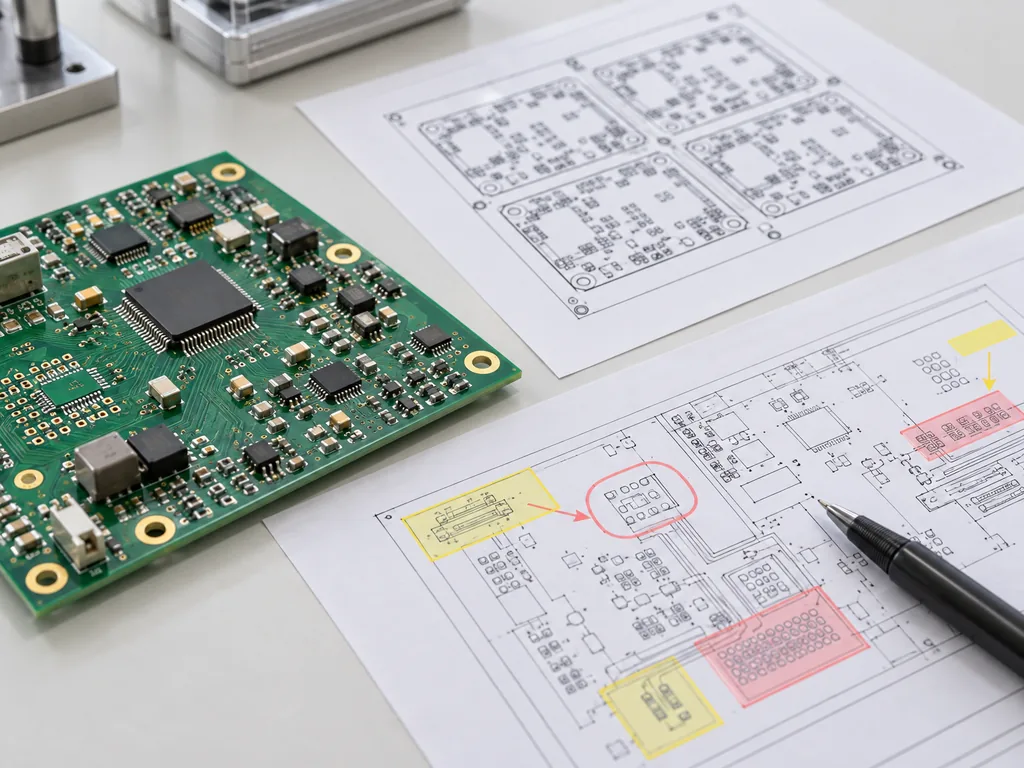
Iteration reduction is not one activity. It is four loops, and each can be tightened independently. A PCBA manufacturing partner shortens all four, but only when the engineering interface is real.
1. Pre-quote engineering review
Before you commit to tooling or procurement, the design should be read by someone who owns the process, not only quoted by someone who owns the price. A useful review produces findings ranked by risk, with the specific consequence of each. "Check clearance" is not a finding. "The U3 pad-to-C12 mask clearance is 0.09 mm, below the process minimum, expect solder bridging" is a finding.
For the review scope itself, see our PCB DFM checklist and the assembly-readiness checks in the PCB design for assembly guide.
2. Prototype-to-production learning
A prototype is only valuable if what it teaches carries into production. That requires the same process, the same fixtures where possible, and a written record of every deviation from the intended build.
If the prototype is hand-soldered on a different line and the deviations are undocumented, it has validated the design and told you nothing about the production process. The defect you find at volume then looks like a surprise, when it was actually a documentation gap.
More on that sequence in the prototype PCB assembly guide.
3. Test and inspection strategy designed in
Decide the test strategy while the layout is still open. Test points, probe keep-outs, and a functional test interface cost almost nothing at layout time and a full spin later. Coverage should match the risk, not the budget line: solder paste inspection before reflow, AOI after, X-ray where joints are hidden such as BGAs and QFN thermal pads, and functional test on the real signal path.
Test-point planning is covered in the PCB test point design guide, and the process side sits in quality testing.
4. Sourcing decisions before layout freeze
Component lifecycle, second sources, and package choices are design inputs, not procurement afterthoughts. Run a BOM readiness check before release: manufacturer part number completeness, lifecycle status, minimum order quantity, packaging, and cross-reference sanity.
See component sourcing, the BOM readiness checker, and the sourcing notes in component sourcing for prototyping.
How to control quality risk without slowing the program down
The wrong reflex is to add inspection. Inspection that is not tied to a specific failure mode adds cycle time and reduces nothing.
The right model is to list the failure modes by stage, then let the PCBA manufacturing partner place the cheapest control that catches each one at the earliest stage where it can be caught.
| Risk | Earliest effective control | Cost if caught late |
|---|---|---|
| Wrong part or wrong polarity | BOM and first-article verification, AOI | Rework, or a functional failure in the field |
| Solder paste volume drift | SPI before reflow | Bridges and opens discovered after reflow |
| Hidden joints (BGA, QFN thermal pad) | X-ray against defined accept/reject criteria | Intermittent failures that pass functional test |
| Functional behaviour | Functional test with defined pass/fail | Customer returns |
| Material identity and traceability | Incoming inspection plus lot records | Recall without a defensible containment scope |
Two things are worth pulling out of that table. First, traceability is a loop-reduction tool, not only a compliance artefact. Without lot records, any single defect forces you to treat the entire build as suspect, which is another iteration. Second, targeted controls beat blanket controls: a defined X-ray criterion on hidden joints removes a loop, while inspecting everything a little removes nothing.
The wider process is described in our 6-step quality control process, and the execution side sits under PCB assembly.
Metrics that show a partner is actually reducing iterations
Ask your PCBA manufacturing partner for these numbers. A partner that cannot produce them is managing by reassurance.
| Metric | What it tells you | Warning sign |
|---|---|---|
| DFM and DFA feedback turnaround | Whether engineering input arrives while the design is still flexible | Generic comments, or findings delivered after tooling |
| Share of issues caught before tooling | Whether review actually prevents loops | Findings only surface once stencils are cut |
| First-pass yield at first article | Process control rather than rework capability | Yield quoted only after rework |
| Engineering change orders after release | Design stability and handoff quality | Rising ECO counts blamed on the customer |
| Prototype-to-production defect correlation | Whether learning transfers between builds | New defect classes appearing only at volume |
| Handoff completeness at first submission | Documentation discipline | Repeated requests for the same file |
Programme-level capability and process scope are summarised on the capabilities page.
How to evaluate a PCBA manufacturing partner before you commit
Ask any candidate PCBA manufacturing partner direct, specific questions. Vague answers are the signal, not the content of the answer.
- Engineering interface. Who is my named engineer? What does a DFM report actually contain? How do I raise a process concern mid-build, and who responds?
- Process control. How are reflow profile and paste volume controlled and recorded? What are your accept/reject criteria for X-ray?
- Test. Who writes the test program? Can you support functional test, and on what platform?
- Sourcing. How do you surface lifecycle risk? How are substitute parts proposed and approved?
- Change control. What is the written process for a deviation, and who signs it off?
Treat these as red flags: no named engineer, only a sales contact; DFM feedback that is a generic checklist with no board-specific findings; changes agreed verbally; substitutions made without written approval; no lot traceability; and any version of "we never have defects".
Quote preparation is worth doing before the conversation, since a complete package makes the review meaningful on the first pass. The PCB quote preparation tool walks through the inputs, and you can contact us once the package is ready.
Handoff checklist, making the first iteration count
The goal is simple: hand your PCBA manufacturing partner a package that makes iteration one a real build, not a clarification exercise. Before release, confirm you are sending:
- Gerbers and drill files, plus a stackup drawing with impedance targets;
- a BOM with manufacturer part numbers and explicit DNI and DNP markings;
- a pick-and-place file with rotations and units;
- an assembly drawing with polarity and orientation callouts;
- test requirements, including coverage, fixture needs, and pass/fail criteria;
- mechanical constraints: enclosure, height limits, mounting;
- target volumes and delivery expectations for both prototype and production;
- special processes such as conformal coating, potting, press-fit, and the depanel method.
The PCB fabrication file checklist covers the fabrication side of that package in more detail.
FAQ about reducing design iterations with a PCBA partner
Can a PCBA manufacturing partner eliminate all design iterations? No. First prototypes exist to find problems, and genuine engineering discovery is not waste. The target is to eliminate avoidable iterations: the ones caused by ambiguity, unverified assumptions, and late decisions.
How early should we involve the PCBA manufacturing partner? Before tooling and before the BOM is frozen. Reviewing a finished design still helps, but it is the least valuable moment to do it, because most of the cheap corrections are already off the table.
Does choosing a cheaper PCBA manufacturing partner reduce cost? Only if the iteration count is identical. On a program with schedule risk, one avoided spin usually outweighs the entire per-unit saving.
Is a domestic or nearshore partner always faster? Not automatically. Proximity shortens communication and shipping. It does not shorten lamination, and it does not repair a weak engineering interface.
What single metric should we track? The number of full build-validate loops from design freeze to production release, together with the share of issues caught before tooling. Those two move together and predict schedule better than unit price.
What if our design is already frozen? Ask for a pre-tooling review anyway. Findings still apply to the next revision, and the first production build can be risk-managed with targeted controls instead of broad inspection.
Next step
Iteration count is decided long before the first board is built, mostly in the review, sourcing, and test-planning stages. That is why the cheapest moment to involve a PCBA manufacturing partner is while the design is still flexible.
Send the Gerber files, BOM, and any test requirements through the contact page, and we will return engineering findings ranked by risk before anything is cut or ordered.