
PCB Testing & Inspection
Soldeerpasta Inspectie (SPI) in PCBA: Wat SPI Detecteert Vóór Reflow en Waarom Het Telt
SE
SUNTOP Electronics
2026-05-21
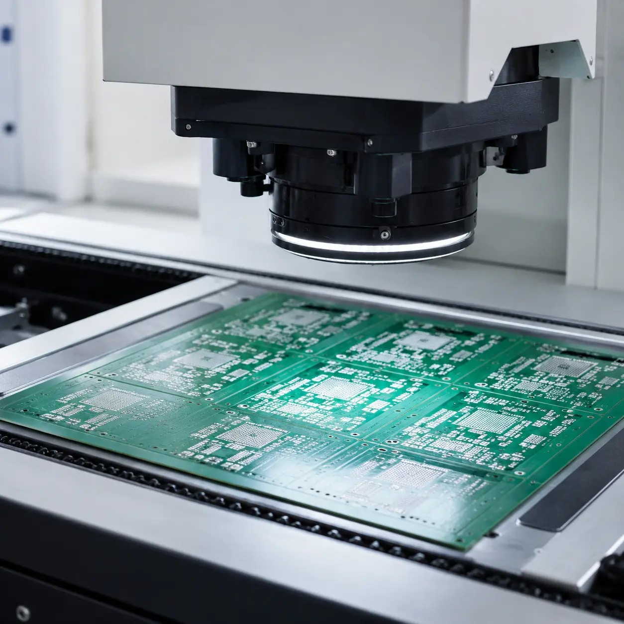
Solder paste inspection (SPI) in PCBA is an essential quality control step executed immediately after stencil printing and prior to component placement and reflow.
What SPI Catches Early
- Insufficient solder paste volume on pads
- Excessive solder paste creating bridging risk
- Offset deposits impacting component alignment
- Clogged stencil apertures causing missing deposits
Combining SPI with AOI and Testing
SPI verifies pre-reflow print quality. It should be combined with AOI inspection post-reflow, alongside ICT or Functional Testing. Compare inspection methods in our ICT vs FCT vs AOI guide.
To discuss your PCBA quality control scope, please reach out via our contact page.
Last updated: 2026-05-21